DIY PRINTED CIRCUIT BOARDS (PCB'S)
After spending beaucoup bucks having PCB's fabricated, I decided to try and make my own. How hard could it be? I did a little research (youtube videos) and decided on the positive acting presensitized circuit board method.
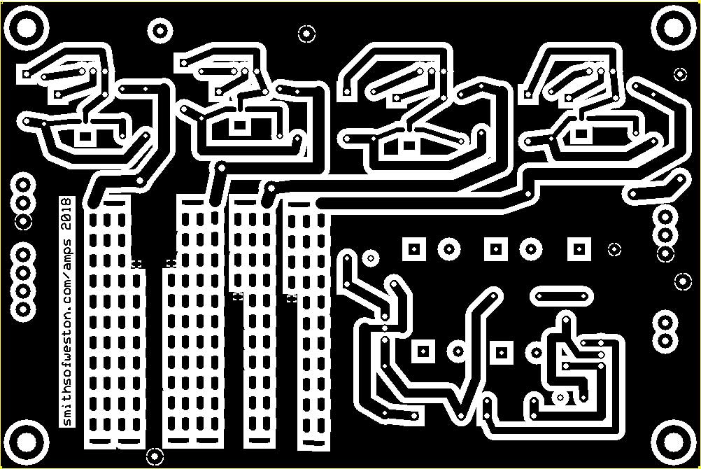
The technique is as follows. Design a PC Board using Eagle or some other CAD program; I use PCB express because it is easy, and my PC Boards are just not that complicated. A simple one straight off the computer is shown below. The black areas will eventually be exposed copper and the white areas will have the copper etched away with ferric chloride.
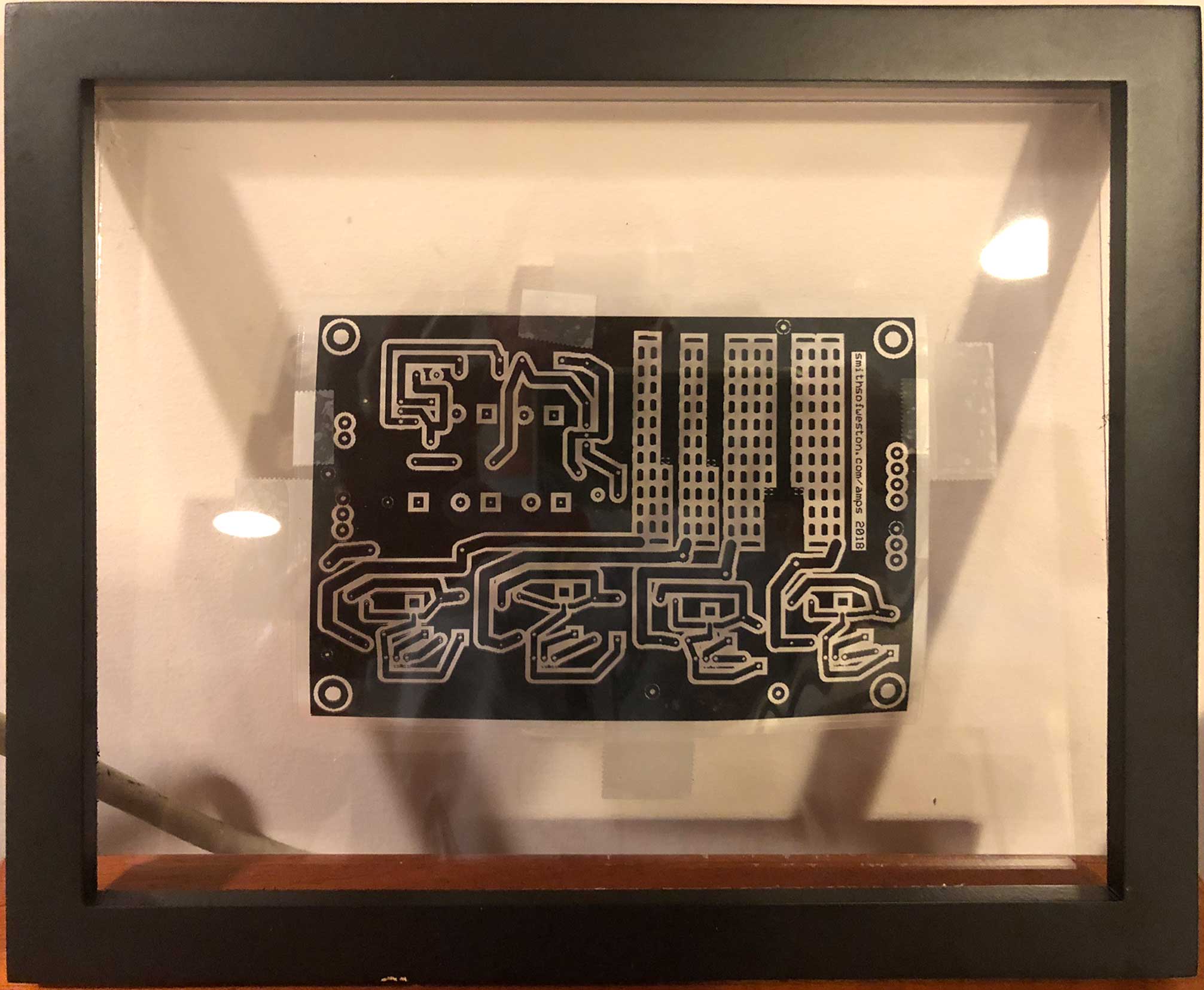
The design is printed out in duplicate on transparency paper and the two identical prints are carefully taped together one on top of the other. This is done to make sure there are not any gaps in the black areas caused by the laser printer. Below I have taped the duplicate printouts to the glass in a cheap frame. The reason for this will be seen below.
The blank PC Board is called a Positive Acting Presensitized circuit board. It comes with a thick copper layer covered entirely with a green layer called a Positive Acting Etch Resistant Sensitizer. This layer protects the copper so that the nasty Ferric Chloride used later cannot eat away the copper.
However, when exposed to ultraviolet light, this layer will soften and can be washed away exposing the copper, which is later eaten away (etched away.) This is where the transparency paper print of the circuit comes in. The areas of the board covered by black will be protected from the light.
In a darkroom (I used a closet with a red headlamp) I carefully peel away the cover on the PC board and tape it so that it lines up with the transparency paper design taped to the picture frame. I put the back cover on the frame to keep the PC board and transparency paper pressed firmly against the glass.
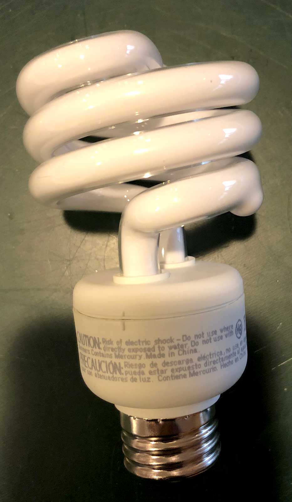
I then expose it to light. A landlord's bulb provides sufficient light to do the job
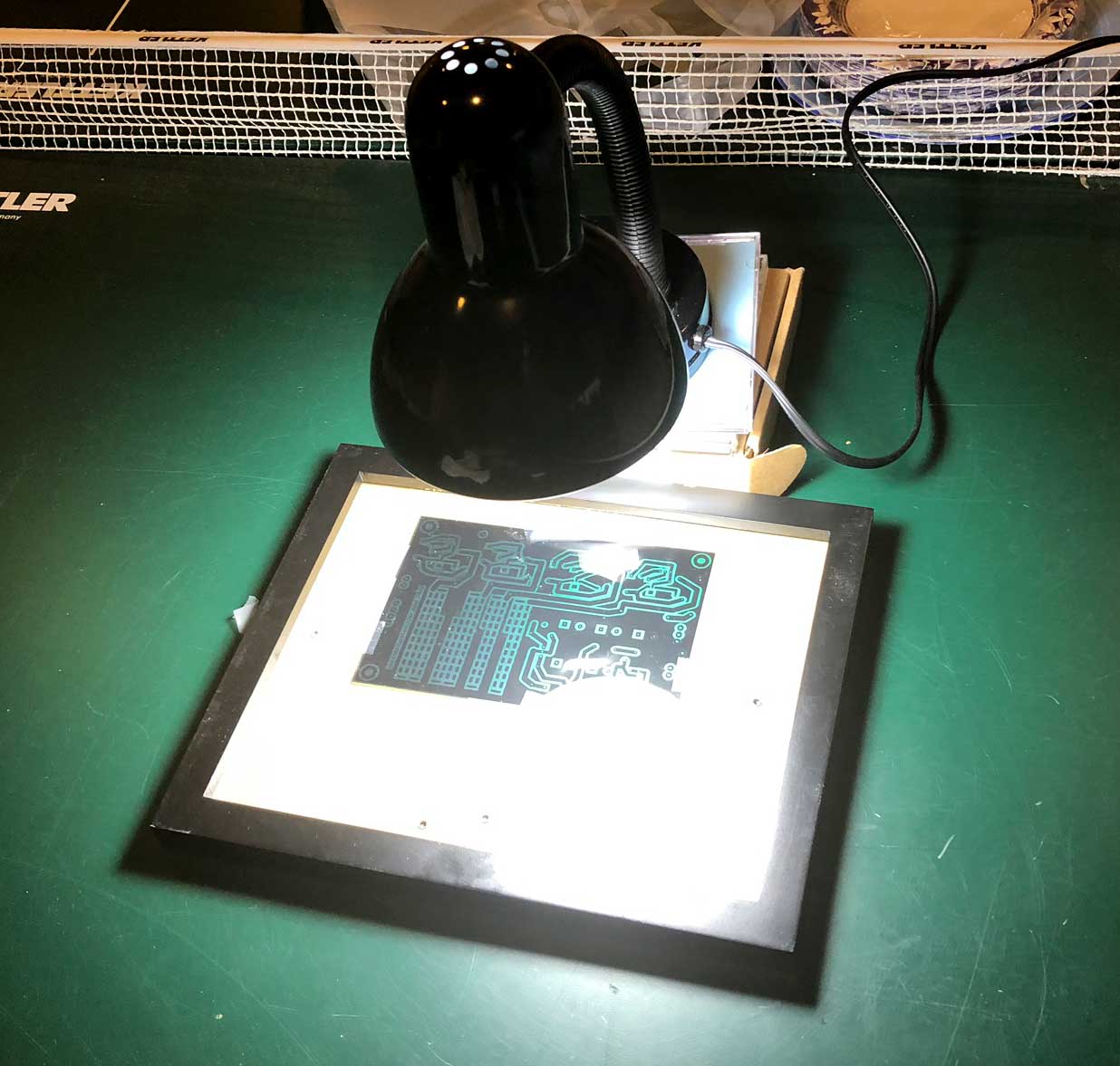
I have found that 10 minutes exposure at a distance of around 6 inches works fine. This is shown below. You can see the green PC board showing through the transparent areas.
The green layer of the PC Board can be seen through the transparency paper below. This is being hammered by the light. The rest of the board is protected by the black ink. The important ping-pong net can be seen behind the setup.
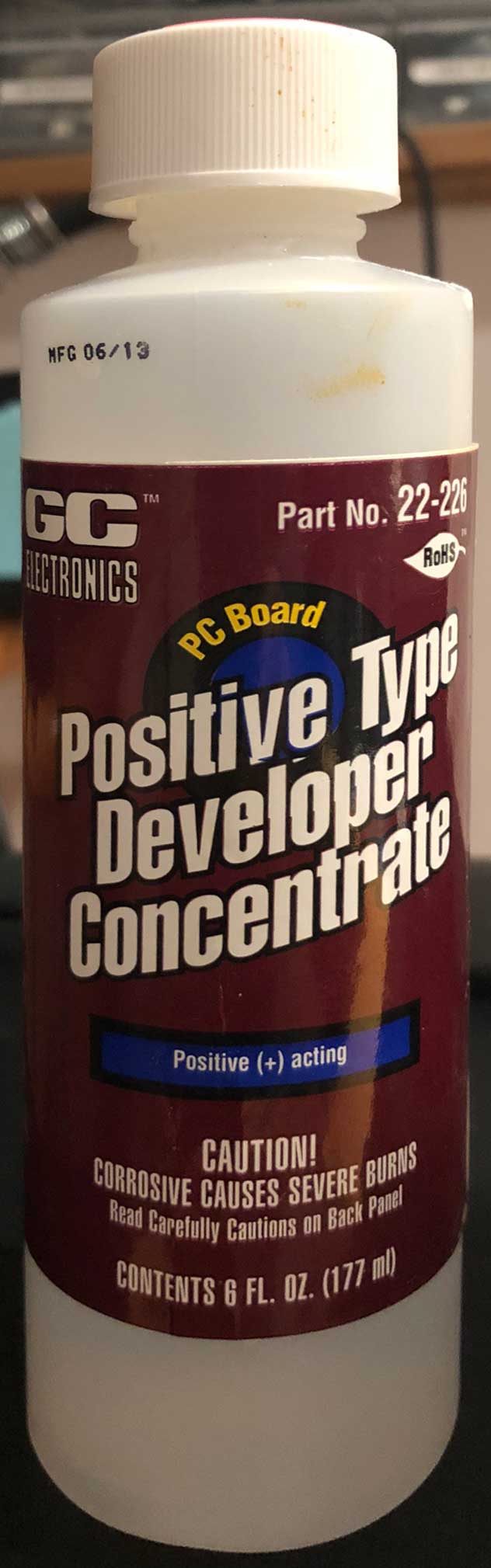
After 10 minutes, the board is taken off the frame and thrown immediately in a bath of positive developer.
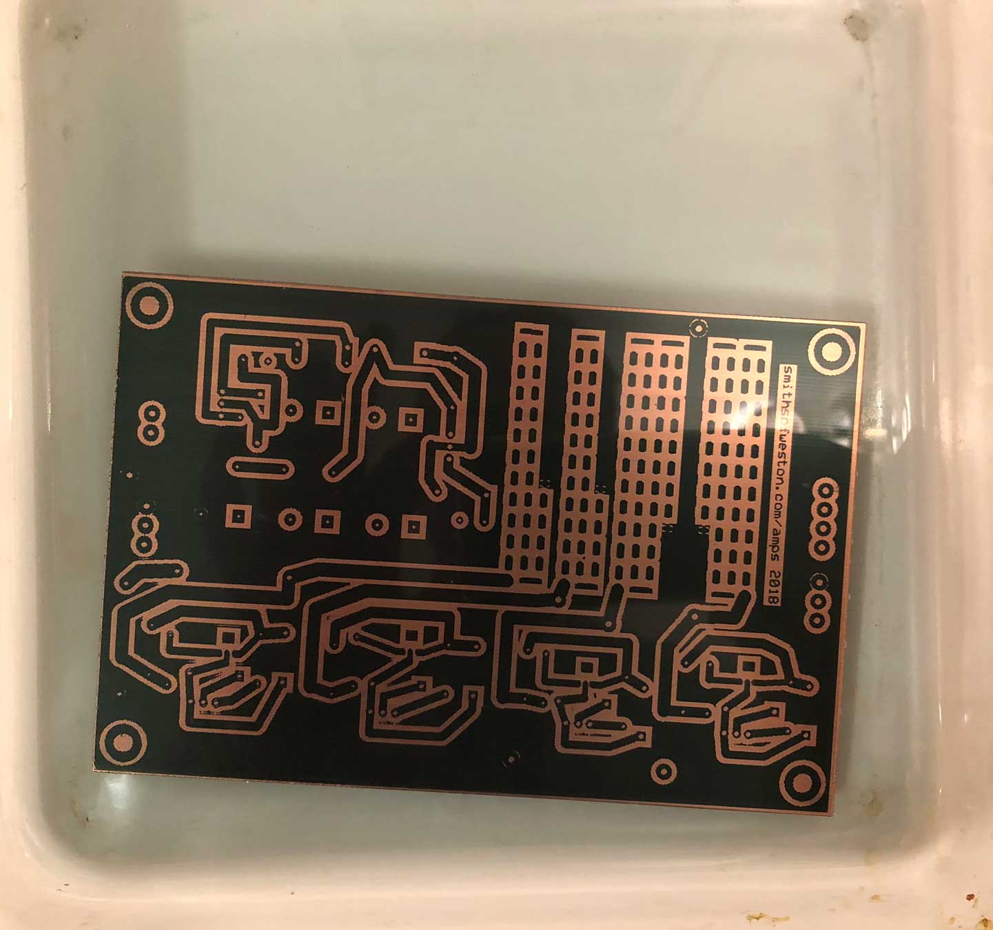
Below you can see the board after a few minutes in the developer. Notice that all the areas that were not protected by black (hence exposed to light) have lost all the green protective goo and are now just exposed copper. Later the board will be put in a ferric chloride bath where this exposed copper will be etched away.
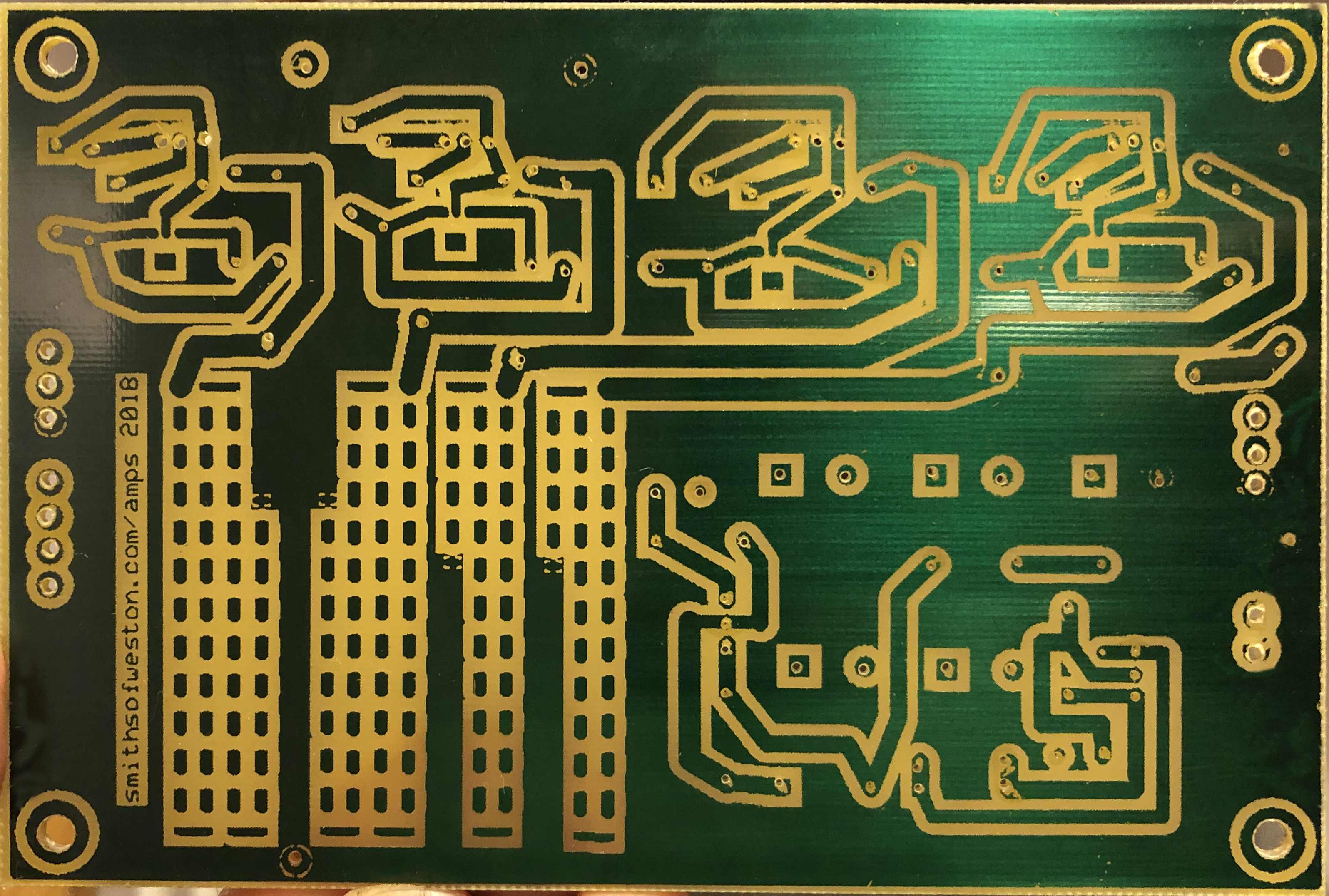
OK, after more than 30 minutes in the Ferric Chloride bath, all the exposed copper is removed and what you see is just green protective layer and the yellowish bare board material.
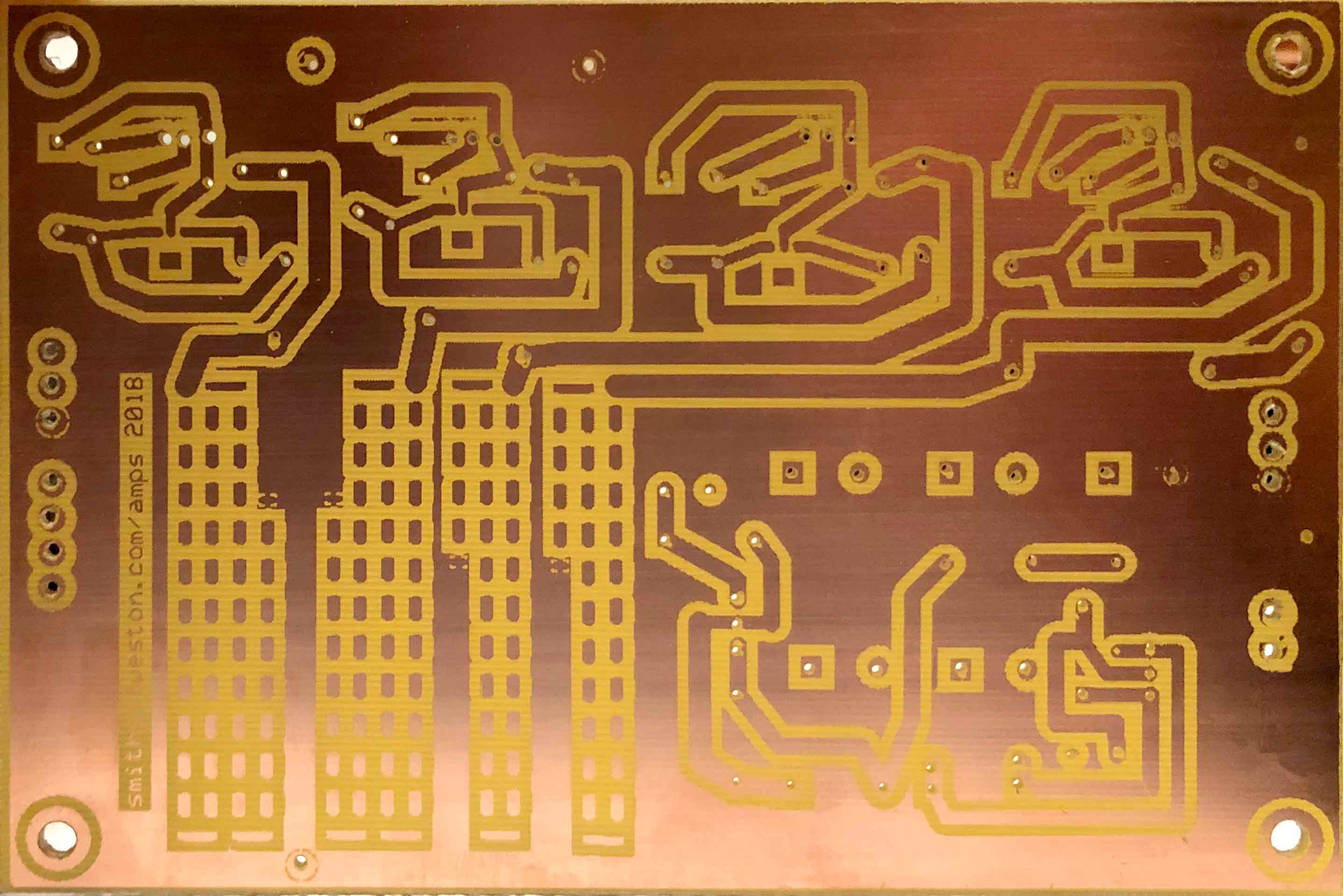
All that remains is to remove the green protective layer with acetone to reveal the beautiful copper underneath.
Ready to populate with parts. Note the very large ground plane.