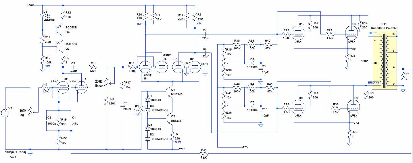
KT90 PARALLEL PUSH-PULL AMPLIFIER
1Feb2018
This is a different configuration of the 70W PPP amp built earlier. The basic audio design will be basically the same, but there is only one choice of feedback: 12dB. It will also incorporate an Arduino microcontroller as in Ben's Unnecessarily Complicated UC6550 amplifier. I have attempted to make this one simpler, with a bit of success.
POWER STAGE
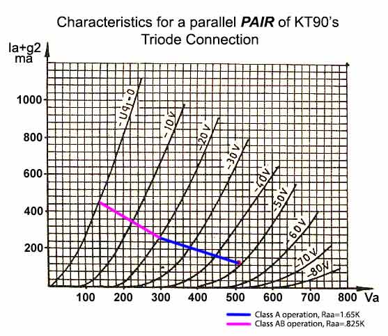
Below are the published curves for KT90's strapped in triode mode. Note that the Ia+g2 axis is doubled for a PAIR of tubes. I have about 500V available from my power transformer, so will use Ia = 130ma. This gives about 32.5W (500 * .065) of dissipation per tube, well under the max of 42W. This operating point is indicated by the red dot. The output transformer has anode-to-anode resistance (Ra-a) of 3.3K.
Looking at the curves, class A operation is marked by the blue line with RL= 1.65K (1/2 of 3.3K). Class B operation (purple line) represents RL= .825K (1/4 of 3.3K)
POWER CALCULATIONS:
Class A1 operation: P = ΔIa2/2 * Ra-a = .132/2 * 3300 = 28W
Class AB operation: P = (2*ΔV)2/2 * Ra-a = (2*(500-140))2/2 * 3300 = 79W
These numbers are unrealistic in real life. In actual measurements, there is no way this amp will make that much power before ridiculous distortion.
INPUT STAGE
Feedback reduces Vin as follows: FB = 20log(Vin/Vgk). So in this case, with FB=12dB and Vi=1.4Vrms,
Vgk = .35Vrms
From above curves (look at the red dot), the grid voltage required by the KT90 power tubes to get full power is about 48Vp (34Vrms). So the amplification required from the input stages leading to the power grids is:
A = 34/.35 = 97.
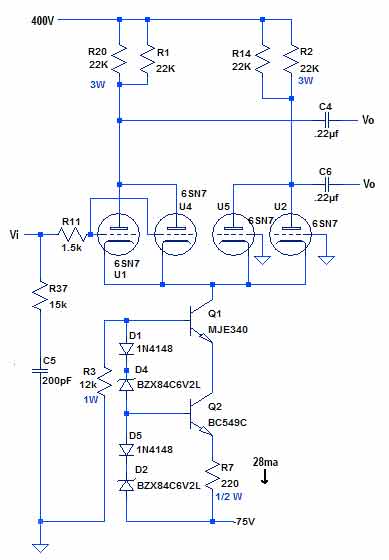
The first stage is a grounded cathode amplifier using paralleled triodes, but with a constant current source (CCS) replacing Ra. 6SL7's will be used.
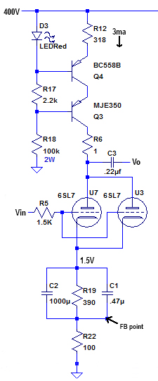
As in my other amps, the constant current source (CCS)is taken from Morgan Jones' "Valve Amplifiers." R12 sets the current at 3ma (1.5ma/triode.) The LED compensates for any temperature variations of Vbe.
This CCS blocks any AC current (since the current NEVER changes from exactly 3 ma). This means that for AC, the anode resistor is infinity (actually about 30-40 Mohm).
The cathode voltage for each of the paralleled triodes is set at approximately 1.5V (490ohms * 3ma). Note that the cathode resistor is divided into 2 resistors, one bypassed by the capacitor. The 100R resistor is the injection point for global negative feedback (GNF).
The gain of a bypassed common cathode amplifier is
A = mu * Ra/(Ra+RL), where Ra = anode resistor, RL = load resistor.
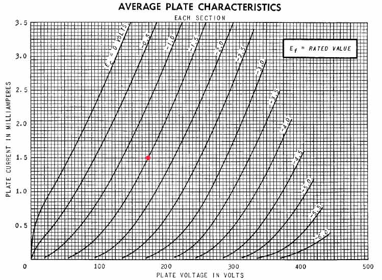
As Ra approaches infinity (possible with the CCS), A approaches mu. The mu of a 6SL7 is about 70, so the gain of this stage should be around 70. In reality it measures out around 60.
Below are the characteristic curves for a 6SL7. The operating point set by the circuit above is indicated by a red dot (I = 1.5ma and Vgk = -1.5V
DIFFERENTIAL AMPLIFIER
A long-tailed splitter generates two waveforms, each 180o out of phase with the other. These are fed into the push-pull power stage.
Paralleled 6SN7's will be used for this stage. Their characteristic curves are shown below. They are extremely linear with Ia > 6ma, according to what I read, and my own testing.
Each tube will have an anode current of 7ma, so the constant current sink in the tail is adjusted to 28ma. The current is set by R7. It turns out that the actual current in the real circuit is around 30ma, so each tube gets around 7.5ma.
Now, for each pair of triodes, Va = 400 - 15ma*22K = 235V, and this is what is actually measured. This operating point is shown below as a red dot.
I designed a printed circuit board to hold the 6SL7 and 6SN7 driver circuits and had it fabricated by ExpressPCB. Miraculously, there were no errors and it functioned properly
Note that 22K anode resistors produce a lot of heat, so they are mounted off the circuit board on a tag board. The MJE340 transistors also have to drop quite a bit of voltage, so are also mounted off-board on heat sinks.
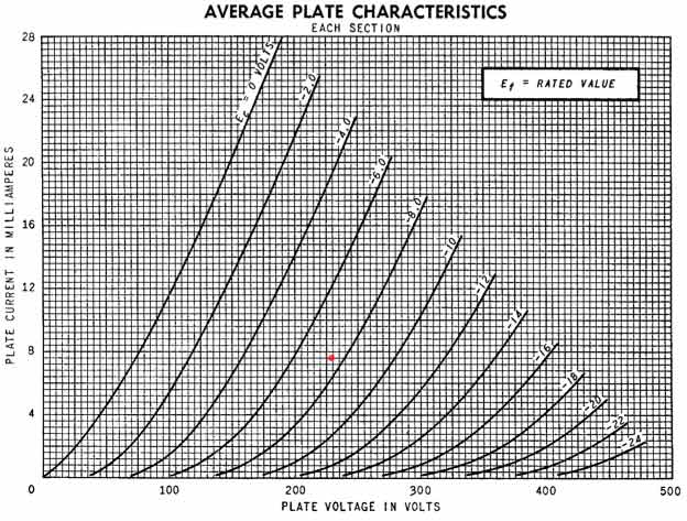
Below are the characteristic curves for the 6SN7 tube. The red dot shows the operating point set by the above circuit. Remember that the 6SN7's are paralleled so the currents are doubled.
BIAS CIRCUTRY
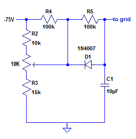
The power tubes will require about -48Vdc applied to each grid. The bias circuit for a single tube is shown here; there are four of these in the amp. These will be point-to-point wired so no PCB is necessary.
The bias for each power tube will be controllable from the front panel of the chassis by 4 10K potentiometers, shown in the schematic.
The bias controls the anode current as well as the screen current. Cathode current, an OK estimate for anode current is measured across the 1-ohm cathode resistor shown on the schematic below.
FEEDBACK
I use standard voltage feedback. The feedback is taken off the 4ohm speaker jack and sent back through feedback resistor R34 to the cathode resistor of the first input circuit. This is R22 in the schematic below.
The overall amplification from input to 4 ohm jack is about A = 175. Feedback can be expressed as follows:
FB(in dB) = 20log(A'/A)
where A is the amplification before FB is applied (open loop FB) and A' is the amplification after feedback.
So, for dB=12, A'/A = .25
The classic feedback equation is:
A' = A / (1 + Aβ)
where β is the feedback fraction.
Solving => β = .017.
Now, β is just the fraction of output that is fed back to the input and is just a simple voltage divider made up of R34 and R22 (100ohms).
β= 100 / (100 + R34)
Solving, R34 = 5700, approximately. A standard 5.6K resistor will be used.
VOLUME CONTROL, BALANCE
The volume control is an ALPS motorized dual-ganged 100K logarithmic potentiometer placed before the first stage. It is mounted on the front panel of the amplifier. Using the teensy arduino and an IR receiver it is remote control. The balance control is a crude affair, consisting of a dual-ganged 250K linear potentiometer between the first and second stages. It is fully manual and should be rarely used, as I have taken pains to make sure that the left and right channel are dead equal.
The entire schematic is shown below. The compensation networks are discussed below.
THE MICROCONTROLLER
Once again, I used the Teensy32 arduino microcontroller. I have revised the PCB a few times so that it is now a general use board that can be used in a number of applications. The schematic is shown below.
I designed the circuit below to be the I/O board for the teensie shown above. There are 12 op-amps contained in 3 LM324 quad packages; these handle the inputs from various parts of the amp; To the right are 9 Darlington buffers contained in a single IC - these output to the power supply relays, the volume control relay, and LED's. The teensy3.2 board is in the center.
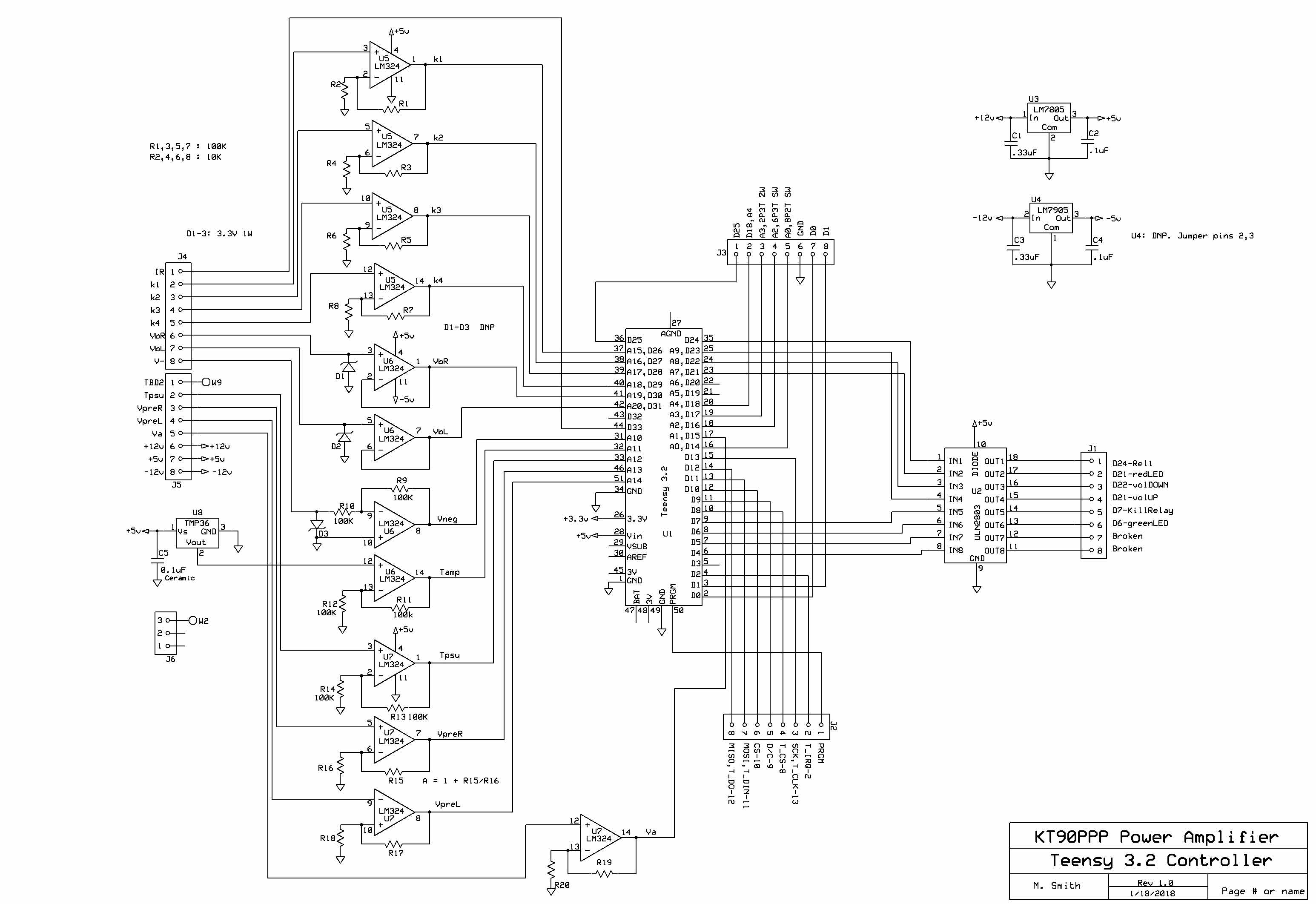
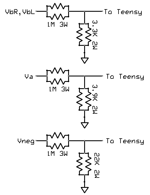
Some of the inputs from the amp are 400-500V. I really don't want these voltages coming on to my delicate little teensy3.2 board, so the little circuits to the left reduce these voltages to appropriate levels for inputting into the op amps that will input into the teensy.
Corrections will be made in the Arduino program.
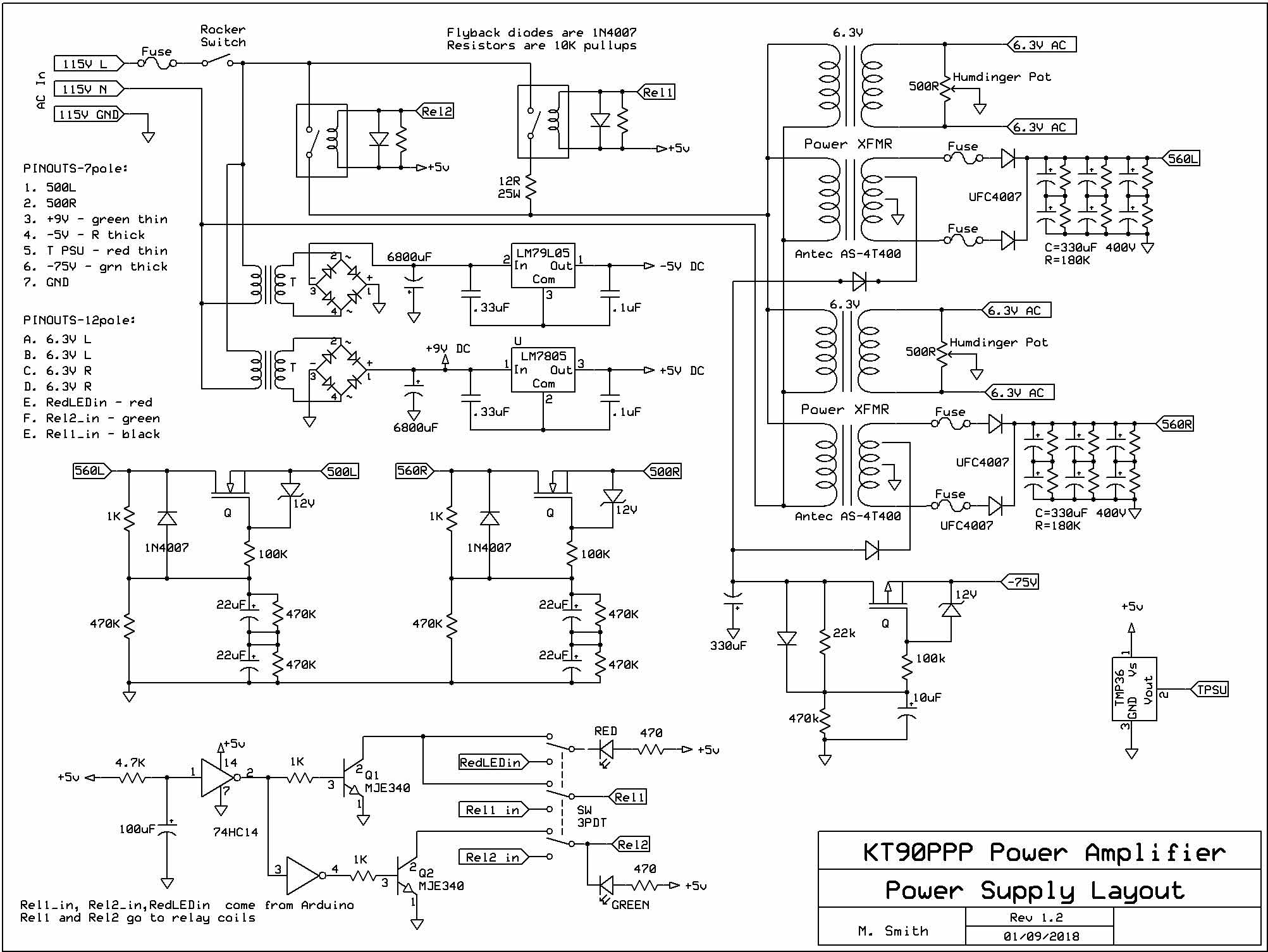
POWER SUPPLY
The power supply consists of the transformers and rectification plus capacitor multipliers sitting in its own chassis plus a voltage regulator sitting in the amplifier chassis. The power supply chassis is connected to the amplifer chassis by a 7-conductor and a 12-conductor power cable. Below is the schematic for the circuitry in the power supply chassis.
Fairly straightforward power supply design. There are 2 relays controlled by the Teensy microcontroller that allow for a soft start. There are 2 positive capacitor mutipliers shown. The n-channel MOSFETs are not labeled but are high voltage, high current devices. There is also a single negative voltage capacitor multiplier. These capacitor multipliers reduce the ripple to a few tens of millivolts instead of the volts that would result from a simple RC power supply. There is a +5V and a -5V regulator, as well as a TMP36 temperature sensor which runs to the microcontroller.
The circuit at the bottom with the 3PDT switch allows the amp to soft-start using the circuitry preceding the switch without the using the microcontroller. Thus the amp is no longer turned off or on by the microcontroller. This is useful during programming when the Teensy is being turned off and on repeatedly as the software is tested. The amp won't turn off and on each time the software is updated, which is frequently, when changes are being made.
Note the rather huge voltages inside the chassis. Approximately 560V DC comes out of the rectifier; this can definitely be lethal.
COMPENSATION NETWORK
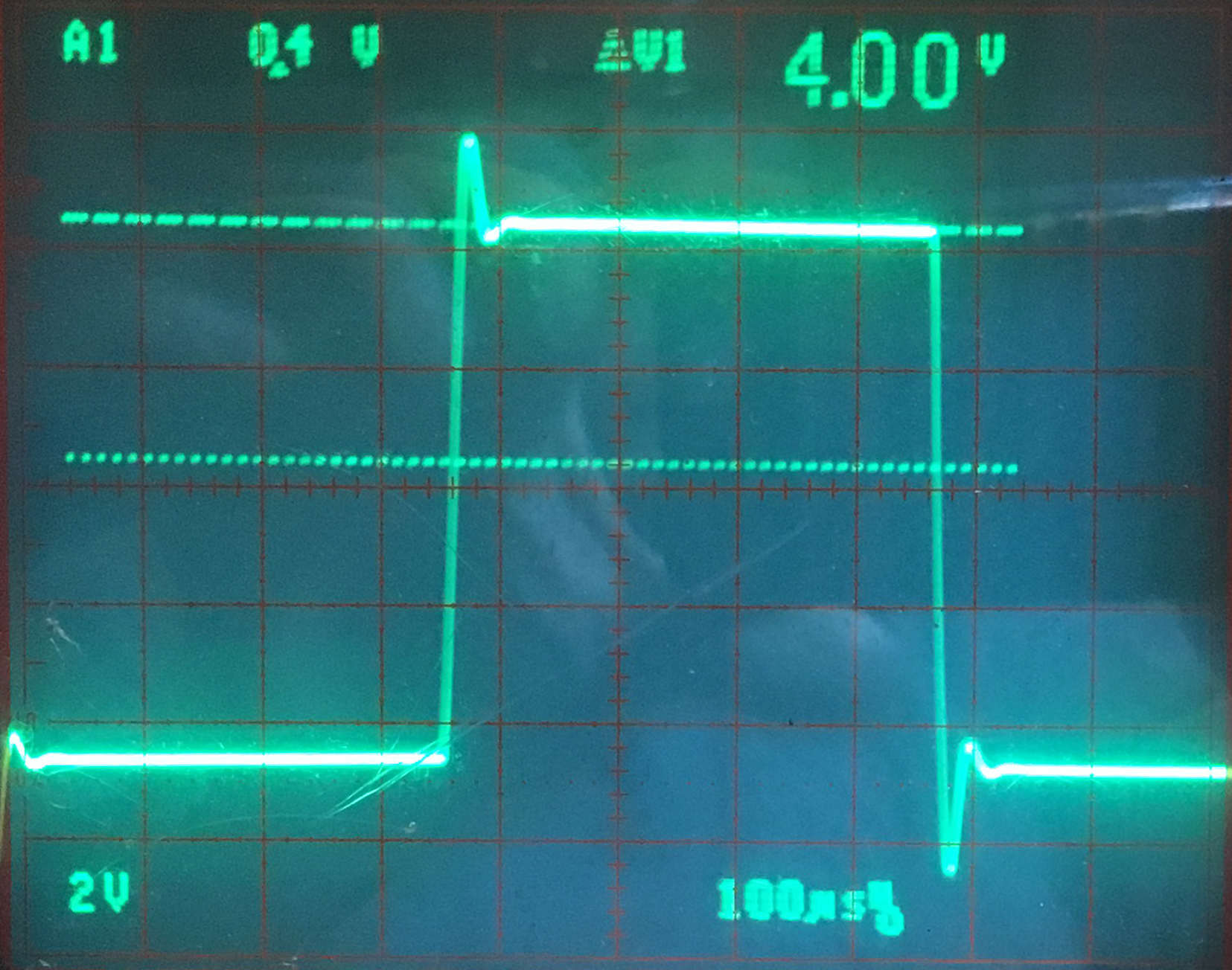
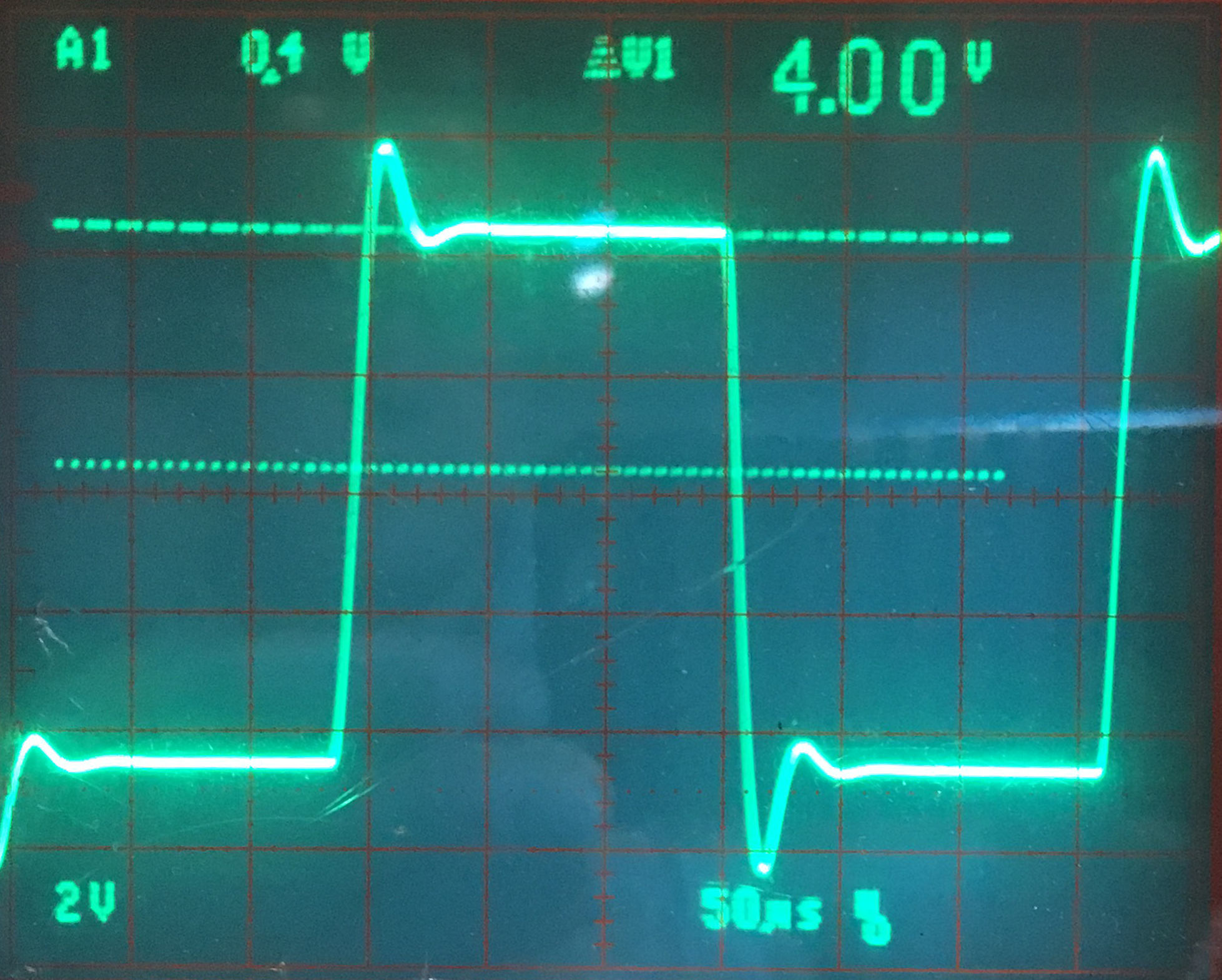
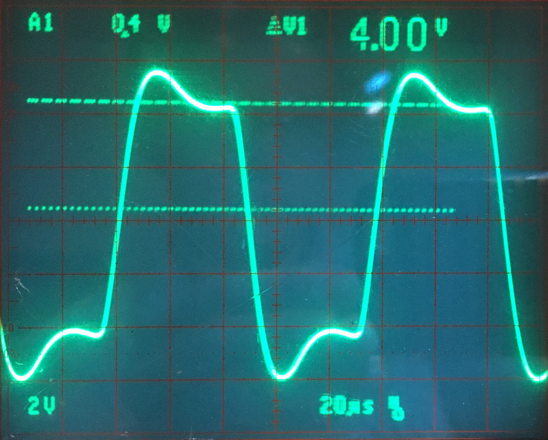
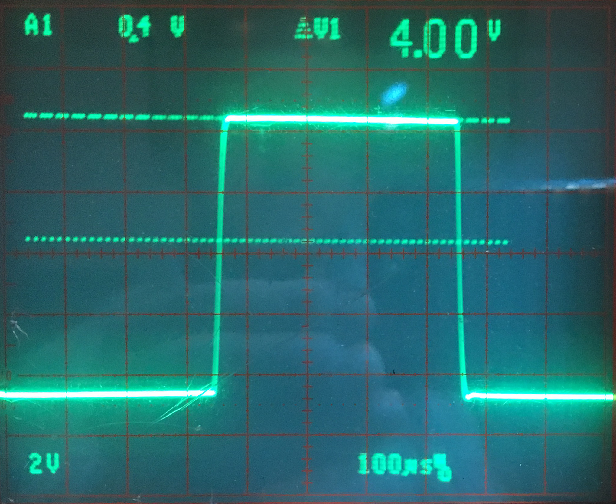
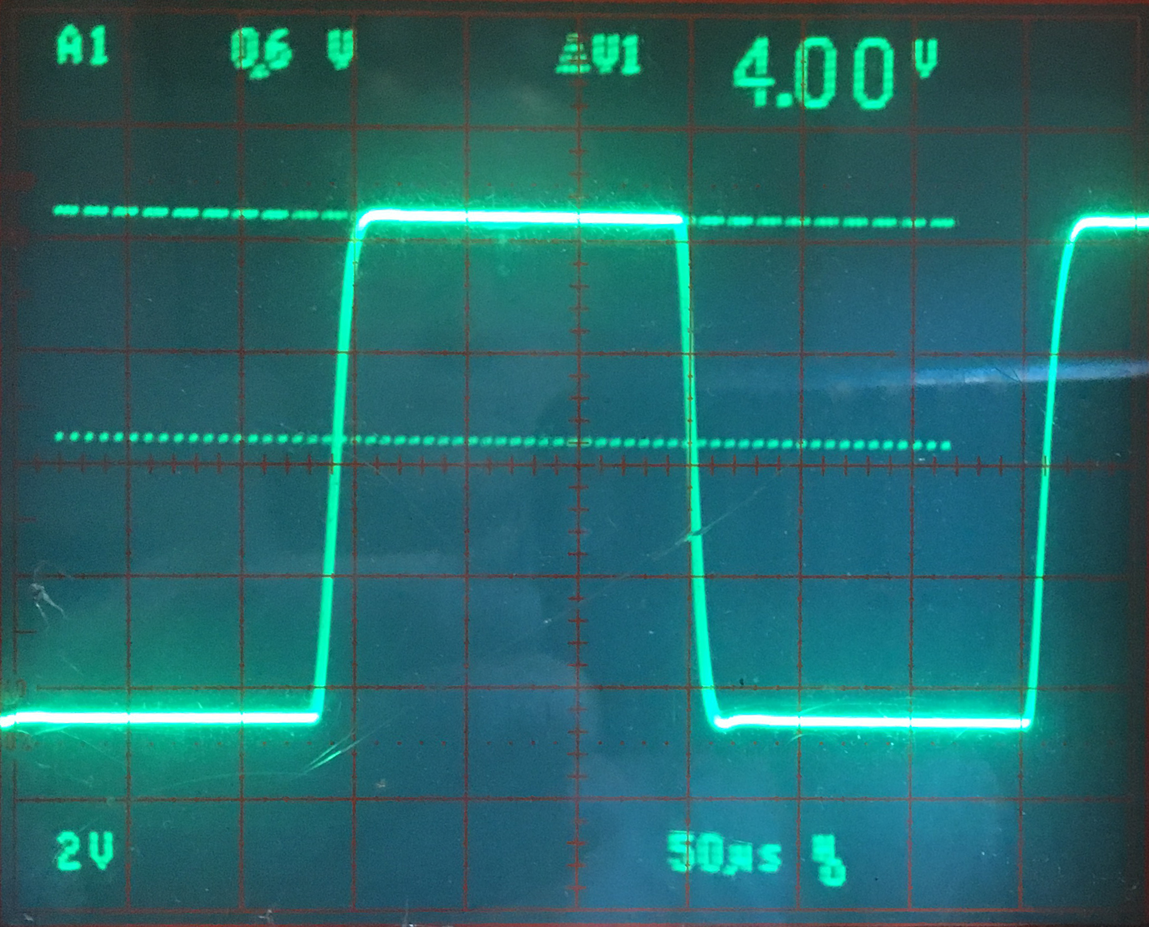
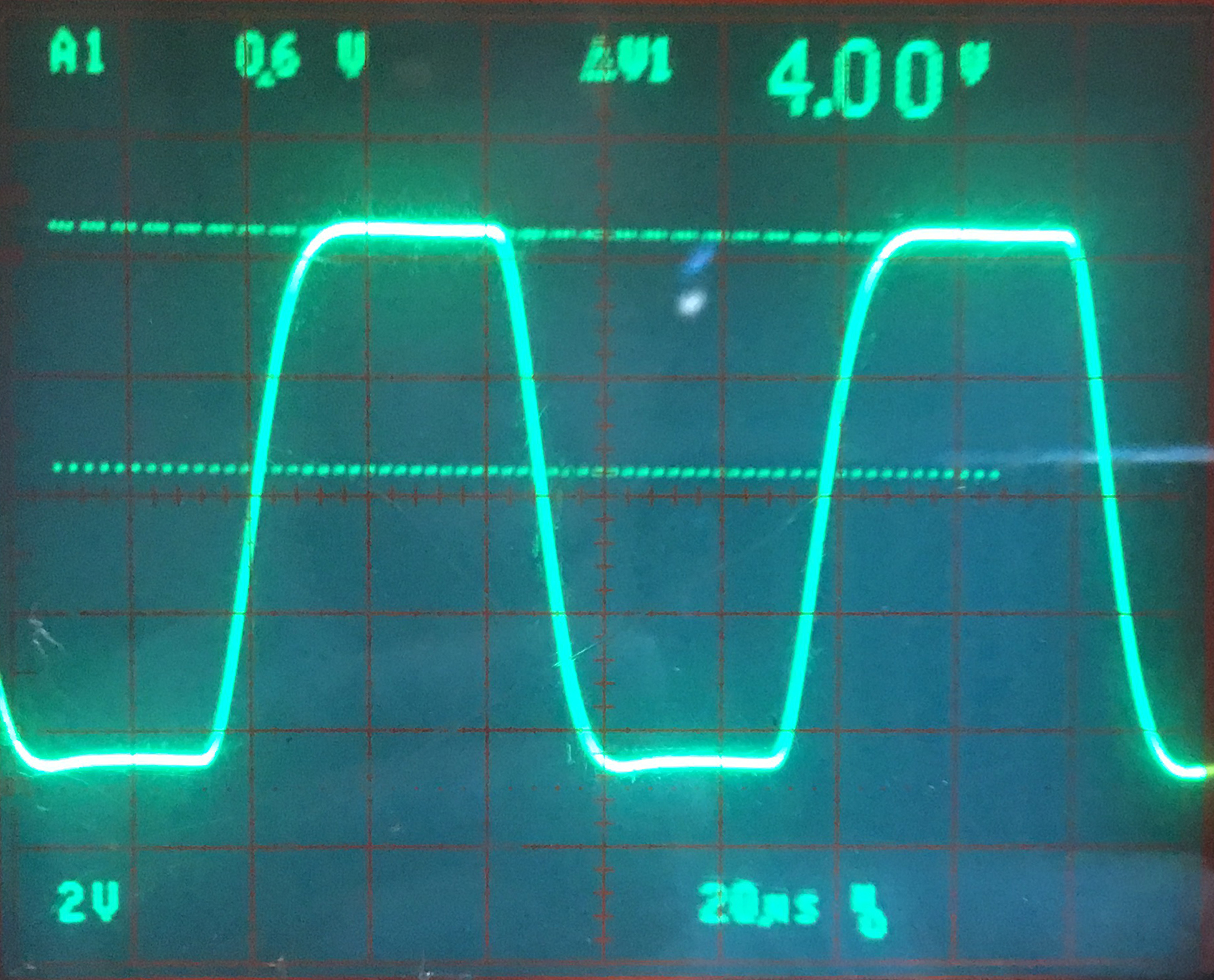
Below are the square wave responses of the of the KT90PPP with feedback. The top 3 are left channel uncompensated 1kz, 3kHz, 10kHz square waves - there is significant ringing on the leading and lagging edge. This means that the amplifier could be unstable at high frequencies without compensation networks put in. All compensation networks are designed to attenuate gain at high frequencies.
1 kHz
3 kHz
10 kHz
Below are the square wave responses with the compensation networks added. These are described below.
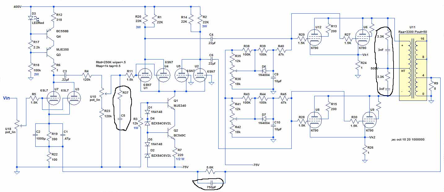
Below is the entire amp with the compensation networks circled. The method I used was taken from a great article by Tim E. Smith on angelfire.com entitled "Empirical implementation of global negative feedback."
The first compensation network is at the output transformer. The technique is taken from Radiotron Designer's Handbook, 4th edition from the 1950's. It recommended a resistor value equal to the Ra-a of the transformer. So 3.3K was chosen. C = 1/(100000*Ra-a) = 3nF.
The next snubber is at the input to the differential amplifier. The values for R37 and C5 are derived entirely empirically. I adjusted a 100K potentiometer and a variable capacitor to eliminate the ringing with the least amount of high frequency attenuation. It turns out that I got satisfactory compensation without this network at all, so it was omitted. In my previous amp, the UC6550, it was included.
Finally, a capacitor is placed across the feedback resistor itself. The capacitor is adjusted until the desired effect is achieved. The idea here is to reduce the impedance of the feedback network at high frequencies, thereby increasing the feedback and reducing gain.
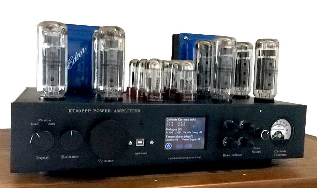
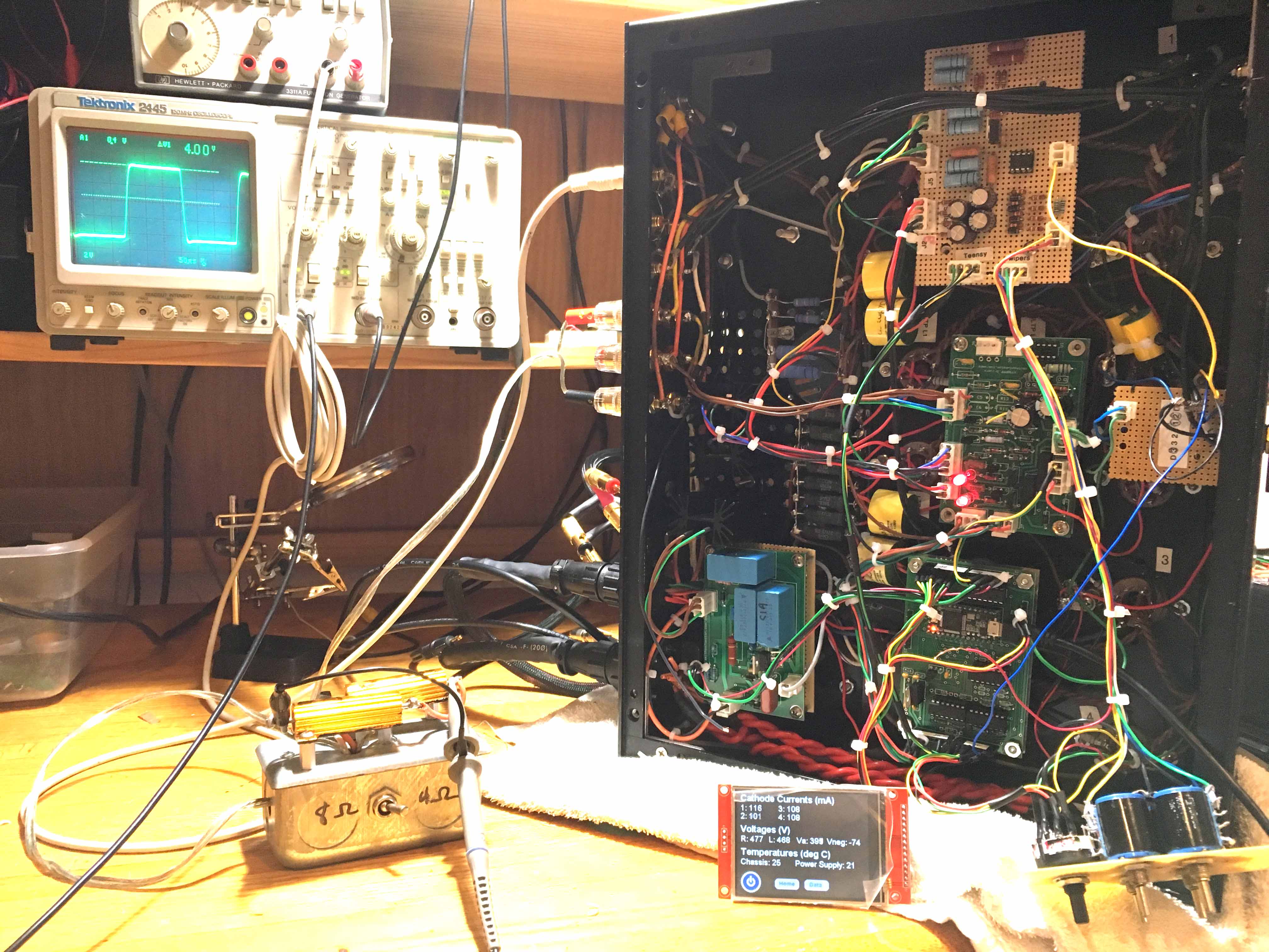
Below is the amp under test. The homemade 4/8 ohm dummy load is connected to the left speaker output. My front panel has not arrived yet, so the screen and bias potentiometers are just laying on the desk.
DISTORTION MEASUREMENTS
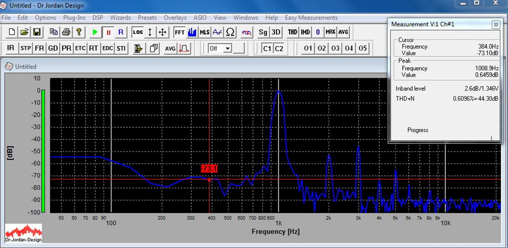
Using Dr. Jordan's WinAudioMLS audio analyzer software, FFT's (fast fourier transforms) were obtained for various power settings. The right channel is basically identical to the left so only the left is shown.
Left Channel at 3 watts - approximately .2% THD+N
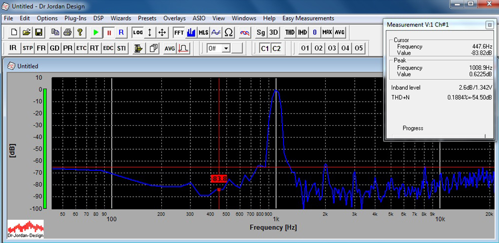
Left Channel at 10 watts - still approximately .2% THD+N
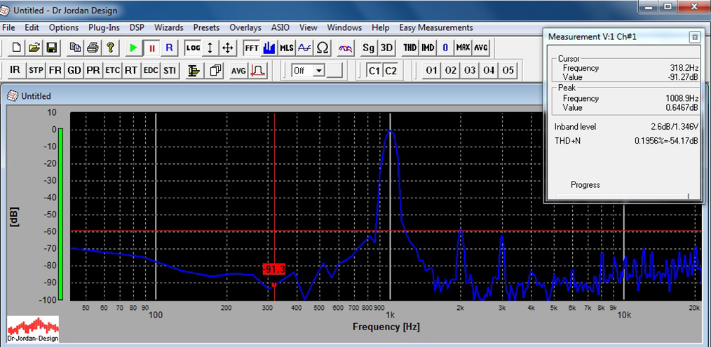
Left Channel at 40 watts - approximately .6% THD+N