70W PUSH-PULL AMPLIFIER
27November2014
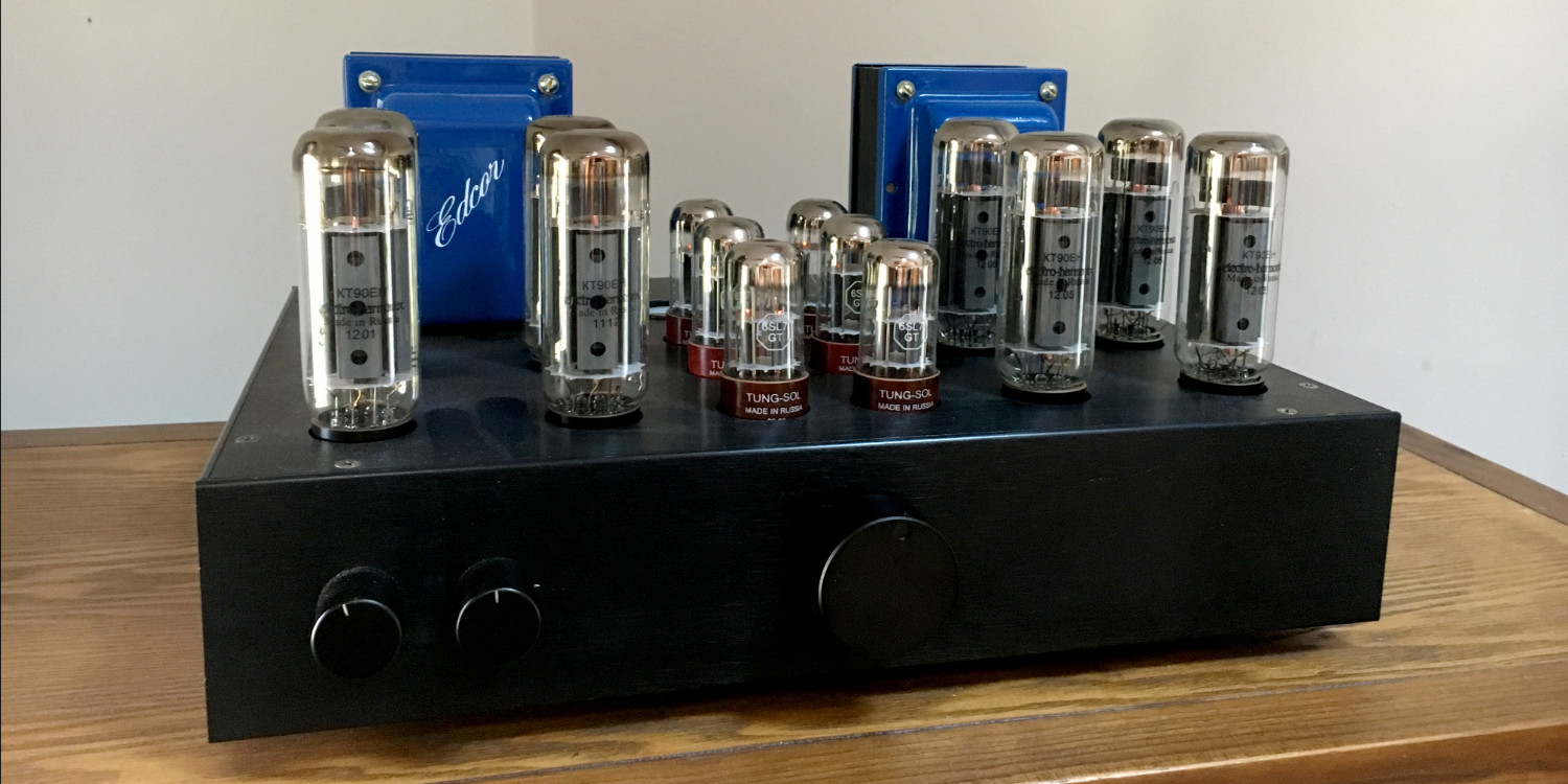
This is my 2nd amplifier and is entirely my design. It is designed to drive more modern (and more inefficient) speakers. The front panel has not been completed. The power supply is separate and not shown. The power tubes are KT90 tetrodes, strapped in triode mode, run in parallel push pull mode. There is just over 500V available from the PSU to power them.
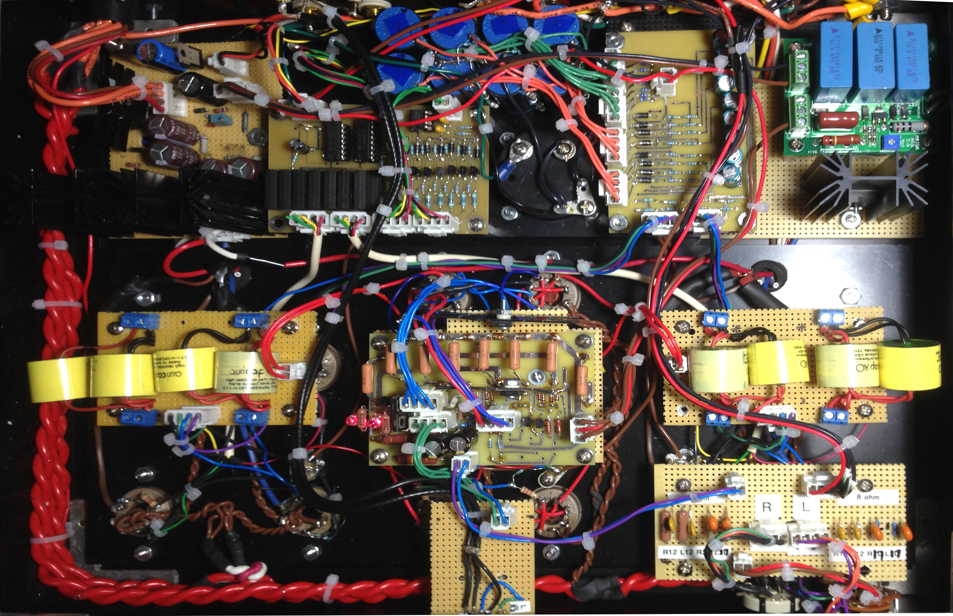
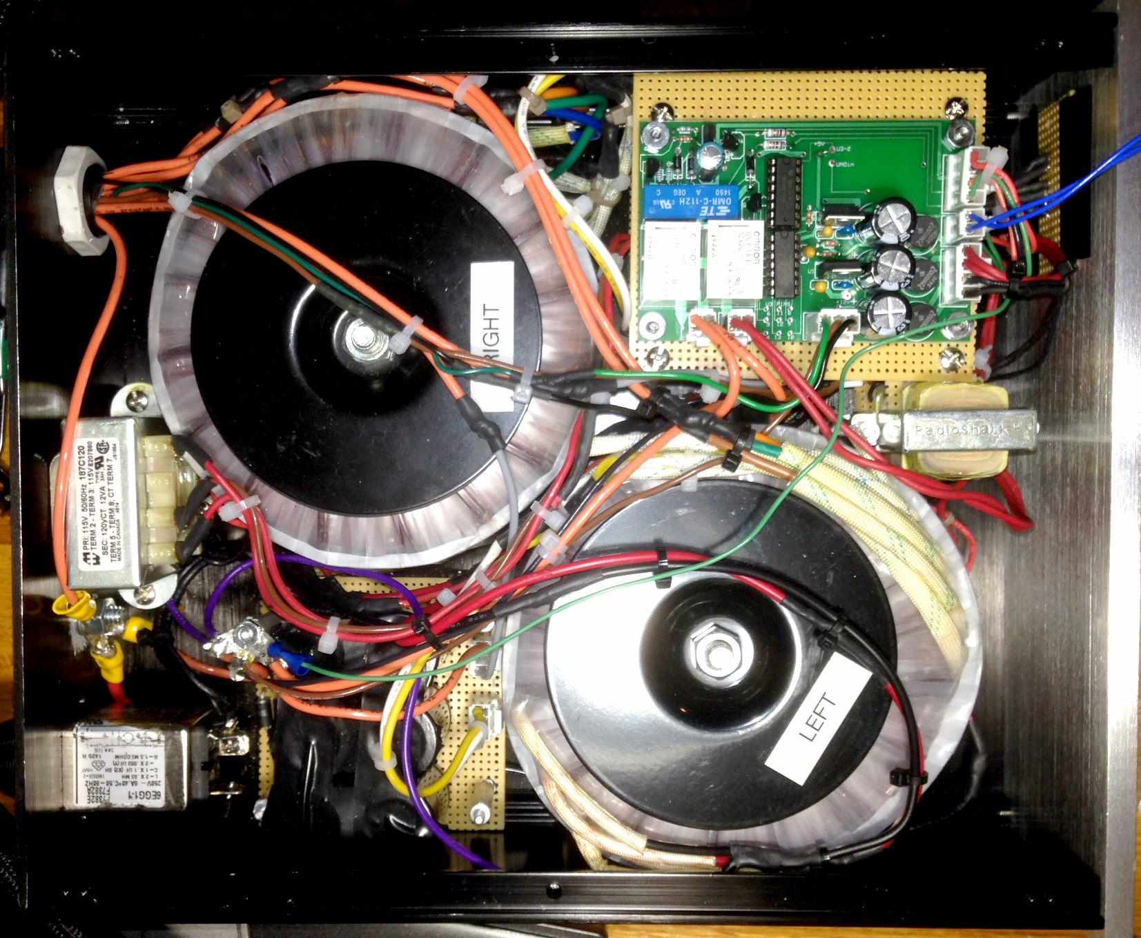
Below is the inside of the completed chassis. No expense has been spared (ugh) - each of the 8 yellow audiophool capacitors is $16. Between the 2 capacitor boards is the board for the driver circuits; note the glowing LED's. In the upper left corner are the "capacitor multipliers" described later, that condition two channels of 500V and one channel of -80V to attain negligible ripple. In the upper right corner is a commercially bought power supply board from Tom Christianson that supplies a regulated 400V to the driver tubes. In the center back are the bias adjustment pots and associated circuitry, as well as the ammeter. All of the boards except for the 400V regulated board were designed by moi.
There is a lot of point-to-point wiring in addition to the circuit boards. The gigantic twisted red wires and the smaller brown twisted wires carry 6.3Vac to the tube filaments.
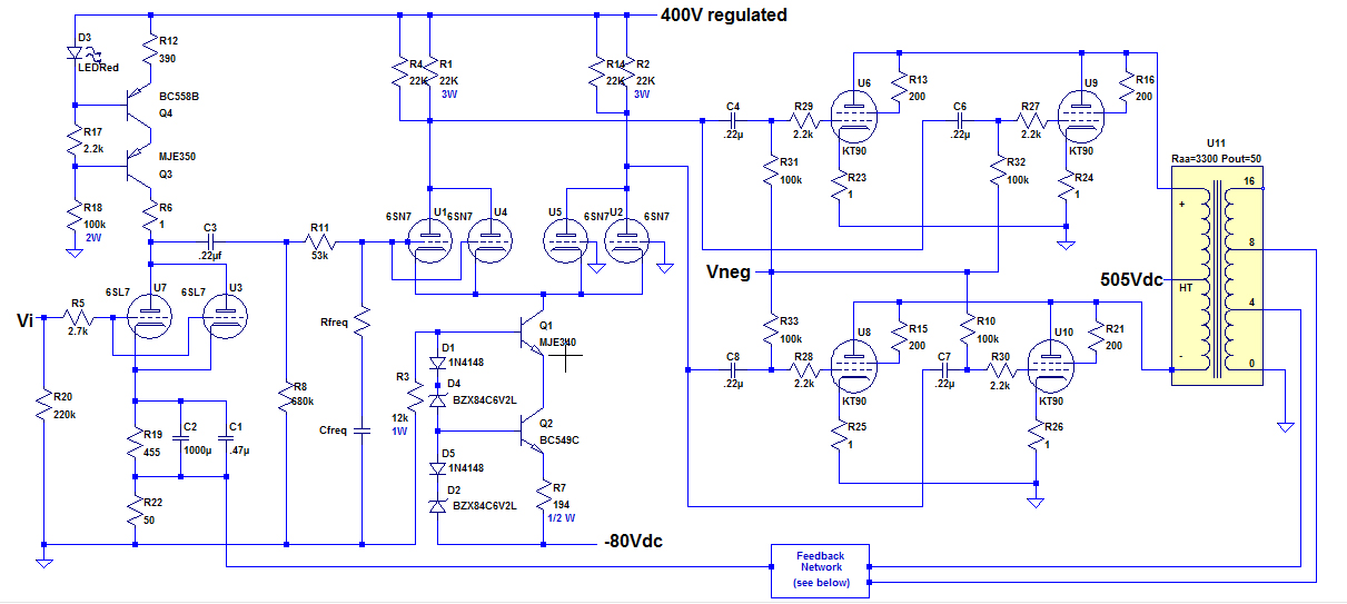
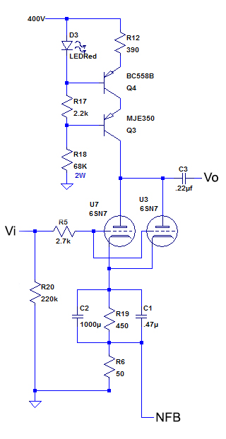
The schematic for the guts of the amplifier is shown below. Note that this is only one channel. It is simply a common cathode input stage followed by a long-tailed pair differential stage, followed by the power tubes.
POWER STAGE
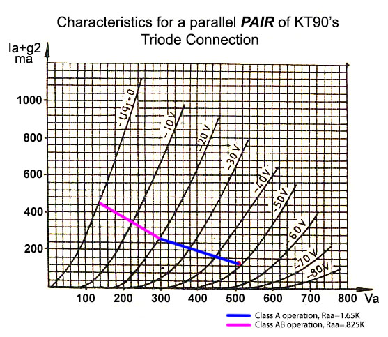
The operating point Q (red dot below) was set at Ia = 130ma (65ma for each tube) and Vak = 505V. Each KT90 must dissipate 505*.065=33W at idle. This is easily under the maximum Pda of 50W for the KT90. However, 8 tubes must dissipate 264W of power into the air as heat.
The bias voltage, from the curves, is around -50V. This is Vbias in the circuit diagram and is provided by a bias network described later.
The output transformers have anode-anode resistance Ra-a = 3.3K. Class A operation is shown by the blue loadline which represents an RL of 1.65K (1/2 Ra-a). Class B operation begins at 2XIa = 260ma and is shown by the purple loadline. It represents a load line of .825K (1/4 Ra-a).
Vg1 (Ug1 on the graph) will never be allowed to go below 0 (or grid current will occur), so the load line ends at the Ug1=0 line. This occurs at Va=140V
POWER CALCULATIONS:
Class A1 operation: P = .5 * Ia2 * Ra-a = .5 * .132 * 3300 = 28W
Class AB operation: P = [2*(505-140)/]2 / Ra-a = 81W
So the amp can theoretically produce 81W in class AB, 28W of class A power. In actual measurements, about 50W is the maximum amount of continuous power I can get - see below. The maximum input signal from the input stages to the KT90 grids before grid current starts is approximately 50Vpeak (35V RMS).
Global negative feedback (GNF) will be taken from the secondary of the output transformer. The voltage across each half of the primary of the output transformer, at maximum power, from the curves above is Vp = 505-140 = 365V, so the peak voltage across the whole primary is 730V, or 516Vrms. Assume a 4 ohm speaker across the secondary. Using the formula
(Vp/Vs)2 = (Rp/Rs) gives a voltage across the secondary (at full power):
Vs = 516/sqrt(3300/4) = 18Vrms.
Double check the above calculation:
Ps = Vs2/Rs = 182/4 = 81W, which agrees with calculation from load line. The actual power from this amp, before significant distortion becomes an issue is about 50W (see below.)
INPUT STAGE
For the purpose of calculations I will assume a max Vi = 1.4V RMS (2V peak). With feedback, the actual voltage Vgk at the grid of the first stage is found with the following expression:
FB (in dB) = 20log(Vi/Vgk).
FB=12dB: Vi=1.4 => Vgk = .35Vrms
FB=20dB: Vi=1.4 => Vgk = .14Vrms
From above, the grid voltage required by the KT90 power tubes to get full power is about 50 Vp (35Vrms). So the amplification required from the input stages leading to the power grids is:
FB=12: A = 35/.35 = 100
FB=20: A = 35/.14 = 250
The first stage is a grounded cathode amplifier, but with a constant current source (CCS) replacing Ra. Also, 2 6SL7's will be used in parallel.
The constant current source is from Morgan Jones' "Valve Amplifiers." The voltage across R12 is set by V across the LED (around 1.7V) + Vbe of the PNP transistor (around -.7). The LED compensates for any temperature variations of Vbe.
It turns out that the voltage across R12 is a little less than 1.2V, so the current through R12 = 1.2/.39 = 3.1ma. So each of the 6SL7's gets a little over 1.5ma of anode current.
This CCS blocks any AC current (since the current NEVER changes from 3.1ma). This means that as far as AC is concerned, the anode resistor is infinity.
The gain of a bypassed common cathode amplifier is
A = mu * Ra/(Ra+RL) where Ra = anode resistor, RL = load resistor. As Ra approaches infinity, A approaches mu. The mu of a 6SL7 is about 70, so the gain of this stage should be around 70.
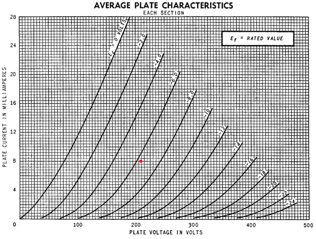
Below are the characteristic curves for a single 6SL7. I am using 2 in parallel.

A pretty linear looking area is around Ia=1.5ma and Vgk (Ef in graph) = -1.5V. This is indicated by the red dot. Remember that the current will be 2 * 1.5ma = 3ma because there are 2 6SL7's in parallel.
By making Vk = 1.5V, Vgk will be -1.5V DC, since Vg is grounded (as far as DC voltage is concerned) through R20.
Rk - the cathode resistor is divided into a 450ohm resistor and a 50 ohm resistor. The top of the 50ohm resistor is the injection point for negative feedback (NFB).
A Spice simulation was done with Vgk=.14Vrms, which is about what it will be at full power and 20db of FB. Vo = 8.8V => A = 63. THD = 0.08%, almost all 2nd harmonic.
The breadboarded circuit, with an input of .1V, had a gain of 63. Using AudioAnalyzer, I measured a THD of .1%, almost all 2nd harmonic.
DIFFERENTIAL AMPLIFIER
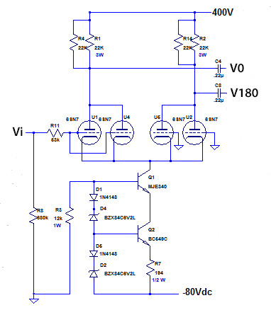
A long-tailed splitter generates two waveforms, each 180o out of phase with the other. These are fed into the push-pull power stage.
The very linear 6SN7's will be used for this stage. Their characteristic curves are shown below. They are most linear with
Ia > 6ma, according to what I read, and my own testing.
Each tube will have an anode current of 8ma, so the constant current sink in the tail is adjusted to 32ma. The constant current sink works as follows: Voltage drop across D5=.7V, across D2=6.2V, across Vbe (Q2)=.7V, so by Kirchoff's Law .7 + 6.2 - V(R7) - .7 = 0. So V across R7 is ALWAYS 6.2V. We can set the current by adjusting R7. R7 is set to 194 ohms, which gives I = 6.2/194 = 32ma, which means 8ma flows through each tube.
The operating point I chose is shown by the red dot. Va here is about 220V
R1 and R2 are 22K, so they each drop 22*8=176V, which means voltage at each anode is 224V. Ok, let's see if it works in LTSpice
Let's see what LT spice thinks of this circuit. Vin is set at .1Vp into the 1st stage. This is a little more than the first stage will be providing at maximum power.
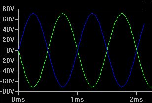
The LT Spice simulations shows pretty decent looking sine waves, 180o out of phase with each other. Note that Vp is around 70V which is well above the maximum that the power tubes can take on their grids before grid current begins.
The FFT (fast fourier transform) is shown below.
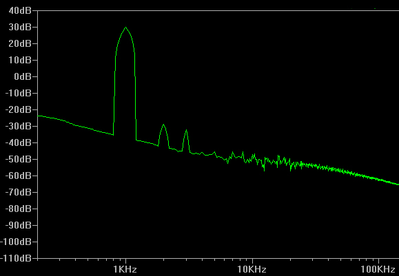
The calculated THD from the FFT is .15% at higher than full power. Note the predominance of 2nd harmonic distortion, typical of triodes, but also the addition of 3rd harmonic, typical of a differential amplifier.
BIAS CIRCUTRY
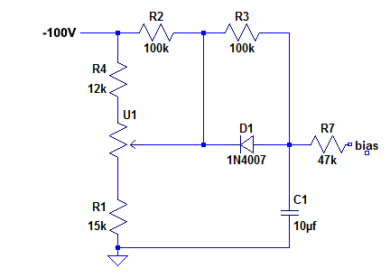
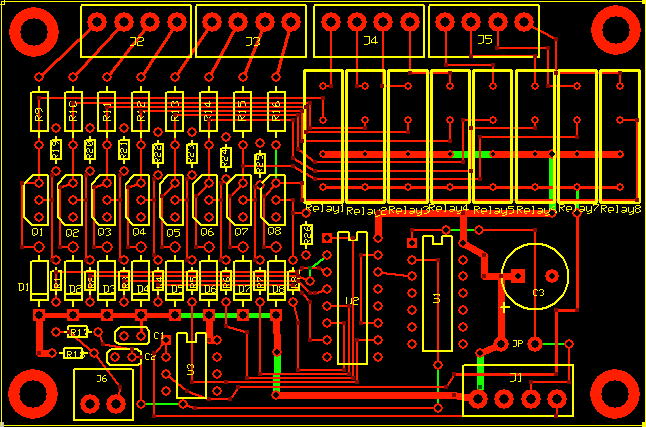
The power tubes will require about -50Vdc applied to each grid. This needs to be adjustable to fine tune and match all 8 tubes. The bias circuit for each tube is shown here. This is reproduced 8 times, once for each tube, and implemented by a PC board designed using the software package PCBExpress.
The bias for each power tube will be controllable from the top of the chassis by 8 potentiometers, shown as U1 in the schematic.
The bias controls the anode current as well as the screen current. It is safest to measure this current by measuring cathode current, and this is accomplished by sticking a 1 ohm resistor in the cathode and measuring voltage across it. I = V/R = V.
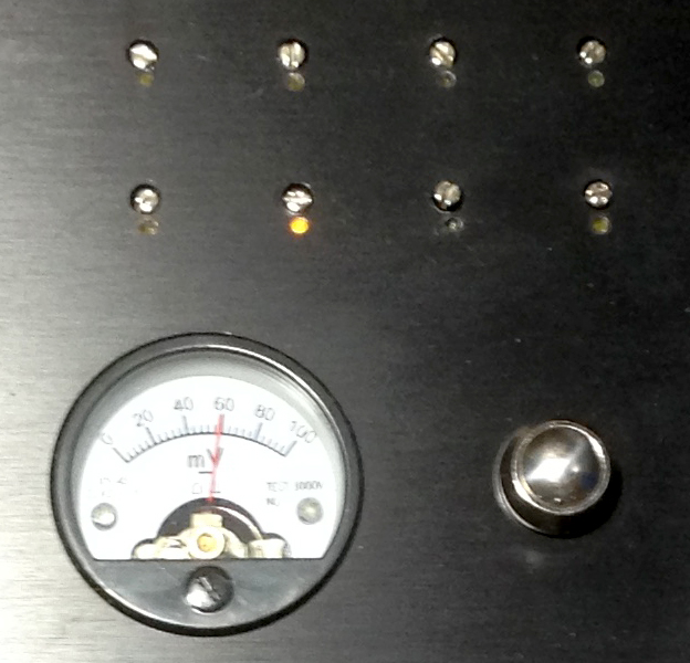
The 8 potentiometer controls on the top of the amplifier are shown. The milliammeter measures the cathode current for the selected tube as the potentiometer is being adjusted. The pushbutton switch is used to select the tube to be measured. The selected tube is indicated by a glowing LED. In this case, tube 4 is selected and the bias is being adjusted to give about 60ma on this tube (60mV across a 1 ohm resistor.)
The pushbutton switch is used to cycle through the 8 tubes. A little logic circuitry was required using a 74HC17 decade counter and some relays, shown below.
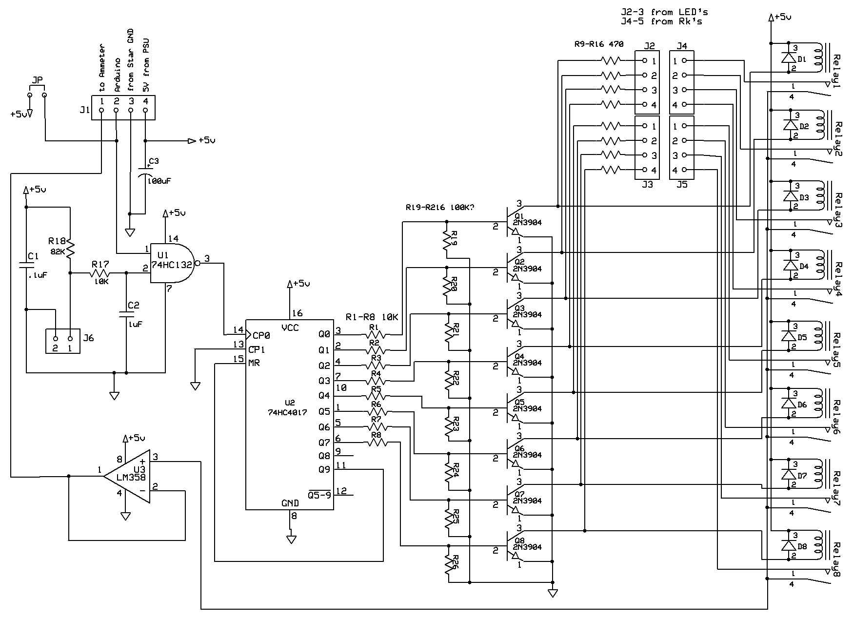
The switch, connected to J6, is pushed and pin 2 of the NAND gate U1 is pulled to ground after being debounced by the RC circuitry preceding the NAND gate. A logical 1 is sent to the decade counter U2 and logical 1 is cycled through Q0 - Q8 with successive pushes of the switch. These outputs turn on the corresponding NPN transistor, which 1)lights the appropriate LED through headers J2,J3, and 2)activates the corresponding relay, which allows measurement of the appropriate cathode current (actually the voltage across the 1 ohm cathode resistor, shown as R23 - R26 in the main amplifier schematic above.) The chosen cathode current measurement is passed through the activated relay to the op amp U3. This is set up to give it a huge input impedance and tiny output impedance which makes it possible to drive the very low resistance ammeter.
This is the PC Board I designed using PCB Express, who accepts the design and fabricates the board. I think it is a competent board. It doesn't have to handle anything too strenuous, and it seems to work. Boo-yah.
FEEDBACK NETWORK
Feedback is derived from the output transformer as shown in the first schematic. The feedback network is shown below. Note that it is backward from the way it is shown above.The 4ohm tap or the 8ohm tap is selected by the 2pole-2position switch on the right.
The 4pole-3position switch selects between 0, 12 and 20dB of feedback. There are thus 4 feedback resistors per channel to select from and their values are calculated and tested below.
I originally designed the amp to have either 12dB or 20dB of feedback, but I could never tame the ringing with a square wave test at 20dB. So I changed the feedback to be either 12dB or 17dB.
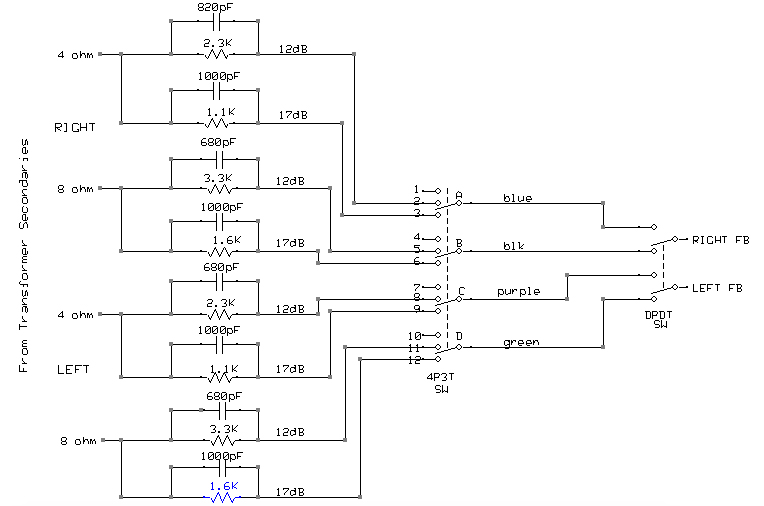
The output labeled RIGHT FB (or LEFT FB) is injected at the top of the 50ohm R22 (see main schematic at top of page). This results in a feedback voltage of:
Vfb = Vo * R22/(R22+Rf).
β is the feedback factor and is defined as:
β = R22/(R22+Rf) where R22 = 50ohms, and Rf is any one of the resistors in the figure to the left.
Rearranging,
Rf = (1 - β) * R22 / β
The feedback equation is A' = A/(1+Aβ), where A' is the closed loop gain, A is the open loop gain, and β is defined above.
Rearranging, β = (A/A'-1)/A
FB in db is defined as follows:
FB (in db) = 20log(A/A')
so A/A' = 10^(FB/20), so:
12dB => A/A' = 4
17dB => A/A' = 7.1
A (open loop gain) was measured at 140 on the 4ohm tap, and 200 on the 8 ohm tap.
Now, Rf can be solved for any amount of feedback:
FREQUENCY COMPENSATION
I don't have the equipment to really test this amp at the high frequencies that produce oscillation. Even with 20dB feedback it sounds good, and my tweeters haven't exploded. But, I'll still put in compensation networks. Tim E. Smith describes an empiric approach that I will use and hope for the best.
The first recommendation is to put a high-pass filter across the output transformer primaries, as shown below. Note that for AC analysis the +505 in the schematic should be replaced with a ground, as the very large filter caps in the power supply are basically shorts to ground for AC signals.
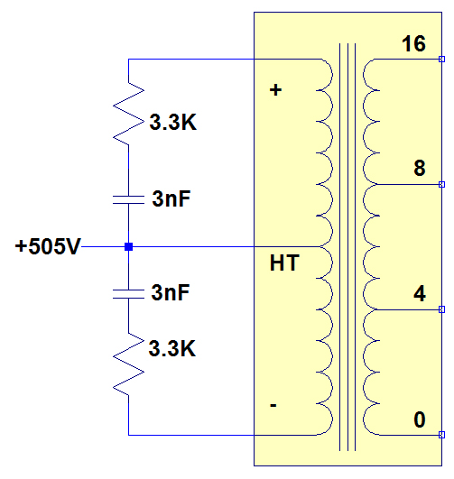
The recommended resistance is the Ra-a of the transformer, which is 3.3k, and the recommended capacitance is 1/(100,000*R) = 3nF.
At a frequency of 1kHz, the impedance across the 3nF cap is 1/(2*pi*1000*3E-9)=53K. However at 100K, the impedance is only 530ohms, so the gain of the amplifier at this frequency is cut significantly. At 250K, the capacitor impedance is 212ohms.
The next step is to put a network at the grid of the differential amplifier. This is shown as Rfreq and Cfreq in the amplifier schematic at the top of the page. Starting with Rfreq=10K and Cfreq=180pF, the best effect on a 2kHz square wave were had with Rfreq=15k and Cfreq=200pF. No improvement was seen by increasing these numbers.
The final compensation is the most important. The capacitors parallel with the feedback resistors were determined experimentally. Using a 2kHz square wave, the ringing was brought under control by increasing the capacitance without causing too much high-frequency rolloff on a 10kHz square wave. The resulting square waves are shown below.
POWER SUPPLY>
I have 2 400V 400VA toroidal transformers from Antek. They weigh 9 pounds each and I need one for each channel.
I use Duncan Munro's excellent power supply design package PSUD2. The circuit for one channel is shown below, which is a simple capacitor with 300ma as the load. The quiescent load for the power supply is the current going to the 4 power tubes at 65ma each plus the current going to the driver tubes, so is probably less than 300ma, but close enough. It is just an estimate.
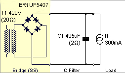
The diodes are ultrafast 1kV rated at 3amps. The 495uF, 800V capacitor is made up of 6 330uF, 400V capacitors. 180K resistors are connected between the positive and negative terminals of each capacitor.
The results of the simulation in PSUD2 is shown below.
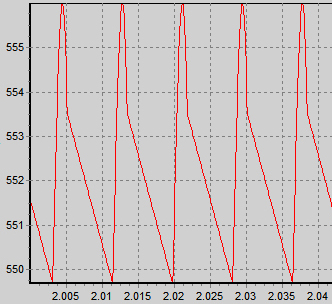
The DC voltage is around 553V with about 6V p-p of ripple. This sucks.
The ripple is unacceptable. I will use a capacitor multiplier to tame this. This is a very cool concept that I first learned about in Merlin Blencowe's great book "Designing Power Supplies for Valve Amplifiers."
The circuit is shown with some modifications below:
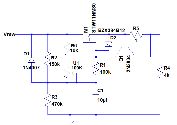
The N-channel MOSFET is set up as a source follower, so the source will try to follow the gate as closely as possible. R2, R6 and U1 form an adjustable resistor between 9K and 63K. The gate voltage is set by the voltage divider formed by this composite resistor and R3 and smoothed by the little cheapie electrolytic capacitor C1. By adjusting U1, Vgs can be adjusted, which controls Vds, hence the output voltage is controlled.
A little note about the 2N3904 transistor and 1ohm resistor. This is a current limiter. As the current increases across R5, Vbe increases in Q1. At .7amps, Vbe=.7 and Q1 is fully turned on, which basically turns off M1. This is just a safety feature. It will not offer very long-lasting protection in the event of a dead short, however. M1 will DIE!
I ran many simulations adjusting U1 until I got an output around 500V. The awesome output is shown below.
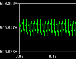
Note that the ripple is now about 7mV p-p, vs 6volts p-p seen above. The output voltage is around 510V. The beautiful thing is that only a little more than a milliamp passes through U1, so a little trimmer potentiometer can be used to control the output voltage of the whole power supply. With U1 at this setting, almost 45V is dropped across the MOSFET and at .3A this means it will have to dissipate around 13-14W. The actual MOSFET I will be using is not modeled in LTSpice but is 950V and 10A, and can dissipate 230W, so this is no problem. It will have to be heatsinked, though.
This is not regulated output, though. The output voltage will vary with line and load variation, but this is not particularly important for the power tubes. For the driver stages, I will use regulated voltage.
The other problem to deal with is inrush current, which is huge with these big capacitors and toroidal transformers. I have turned on the basic power supply with just the single transformer and capacitors and the lights dim in my workshop momentarily. And this is just with one transformer. So an inrush current limiter will need to be used. The basic scheme is shown here.
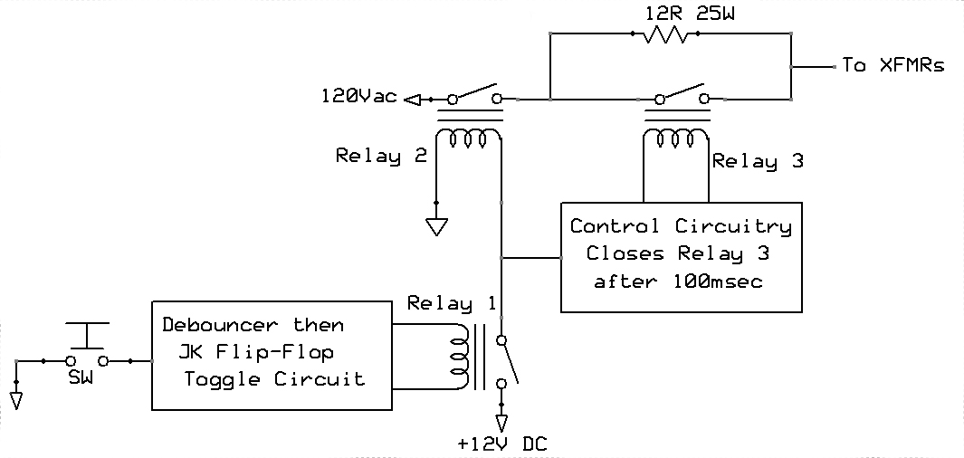
The power switch is a low-voltage normally-open pushbutton switch that looks cool on the front of the power supply chassis, unlike the clunky big power switches seen on most DIY amps. The debounceer-toggle circuit activates relay 1, which sends 12V to the control circuitry and to relay 2. Relay 2 closes and allows 120V to go to the transformers through the big heat-sinked 12 ohm resistor. After 100msec, relay 3 closes, bypassing the resistor.
The control circuitry is just a simple delay circuit shown below:
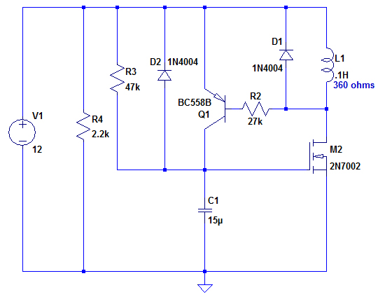
The 12V shown comes off Relay1. C1 starts slowly charging through R3 which causes M2 to start gradually turning on. As M2 starts allowing a little current to flow, Q1 base voltage, initially at 12V, starts to drop. When it drops about .7V, Q1 turns on abruptly and almost instantly charges C1 which fully turns on M2. Current is now flowing through L1 (which is the coil of relay3.)
A SPICE simulation of current through the coil is shown below.
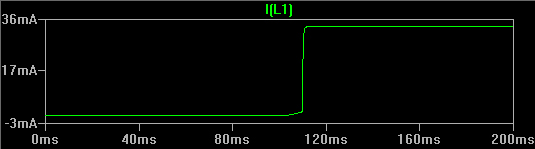
Note how the coil current "snaps" on. This is good. It turns on relay3 at a little past the 100msec mark, which is close enough for government work.
I breadboarded the little delay circuit and measured the delay on my old Tektronix 2445 scope. The probe was placed at the top of C1.
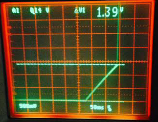
You can see that C1 starts charging slowly, but at about 110-120msec, at 1.39V it snaps and becomes instantly charged, as described above.
I went ahead and breadboarded the power supply with inrush limiter. You can hear the initial relays close, followed by relay3. The 12 ohm power resistor stays cool, and there is no measured voltage across it, proving that all the current is going through relay3. Yay!
Debouncer Circuitry
I used a standard hardware solution for debouncing. I plan to use a normally open pushbutton switch, that is only closed when it is pushed. Even a crappy cheapo like I plan to buy will probably bounce no more than 20msec or so. The following circuit is in LT spice.
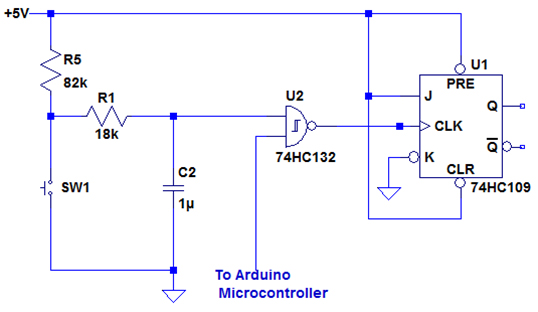
SW1 is a normally open pushbutton switch. The debouncer is just the RC circuit formed by R5, R1, and C2. When the switch is open, the capacitor charges through R5,R1 until 5V is at the input to the Schmitt Trigger NAND gate U2 and the output of U2 is 0. When the switch is pushed, C2 now discharges through R1, and the voltage at U2 drops until at some point, the output of the NAND gate snaps to 1. This should take longer than 20msec to give the switch a chance to finish all it's bouncing. The reason for the NAND gate rather than a simple inverter is that I eventually want to have an IR remote control. I will be using an Arduino Microcontroller in the main amplifier chassis, and when the power button on the remote is pushed, the Arduino will send a logic "0" to the NAND gate.
The circuit is simulated below.
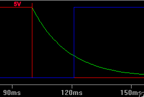
The red trace is the voltage across the switch. It starts at 5V (logical 1) then at 100msec, the button is pushed and the switch goes to ground. This allows the capacitor to discharge, shown by the green trace. At a little over 20msec, the output of the NAND gate U2 (blue) snaps to logical 1. So, at least in LT spice, the switch can bounce and do all the junk it wants to, but nothing will happen until all the bouncing has stopped - hopefully within 20msec.
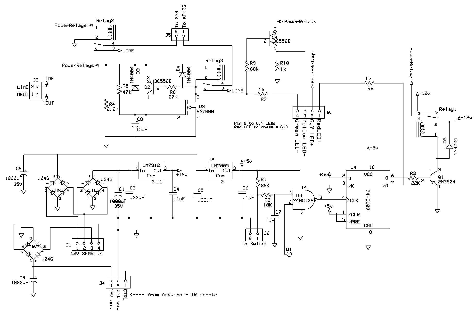
I decided to implement the above with pc boards. Express PCB is a low-cost house that provides free design software. I used ExpressSCH to design the following circuit. It includes the soft-start circuitry at the top, voltage regulators, switch debouncer and toggle software on the bottom.
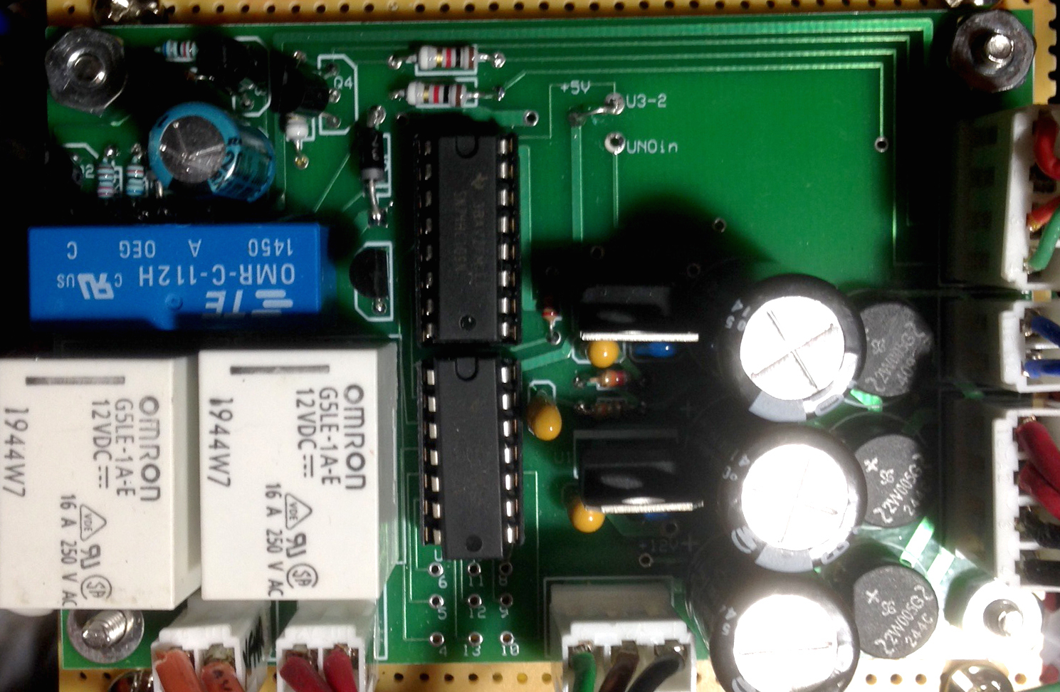
This is the stuffed pc board. You can see the Omron relays at the left.
The interior of the finished power supply.
I built a thick cable to connect the power supply to the amplifier. It's really unwieldy and thicker than my thumb, and frankly ugly, but it works, I suppose.
CHASSIS
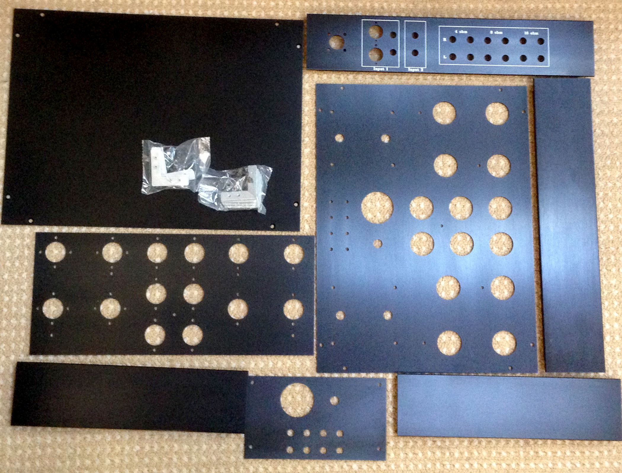
I used Front Panel Designer to design the case, and had the case built by Landfall Systems in Texas. The unassembled pieces are shown here. There were a few bonehead mistakes, but nothing that couldn't be corrected, and only one affected the appearance - in the back where nobody will notice.
HEATER SUPPLY
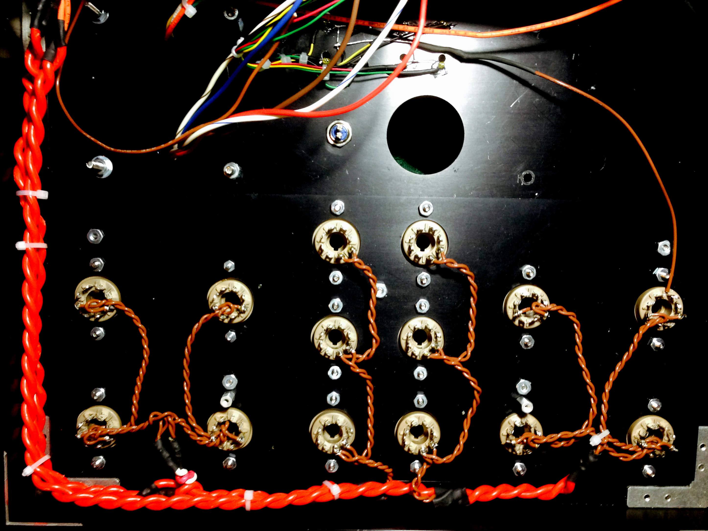
I have decided to use AC for the heaters. Each of the 8 KT90's draw 1.5A to its heater, and each of the 6 driver tubes draws .5A. So there is about 15A going to the heaters. This requires some very thick wire coming from the power supply case. Even if the wire is only .1ohm over its entire length, 1.5V will be dropped from the power supply case to the amplifier case, which is unacceptable. So I used a pair of 12 gauge wires for each channel and kept the power supply cable very short. The final wiring is shown below here.
MEASUREMENTS
According to theory, distortion should be reduced by a factor of (1+Aβ). The open loop gain of this amplifier is A=140.
12dB: β = .021 => distortion should be reduced by factor of 4.
20dB: β = .043 => distortion should be reduced by factor of 7.
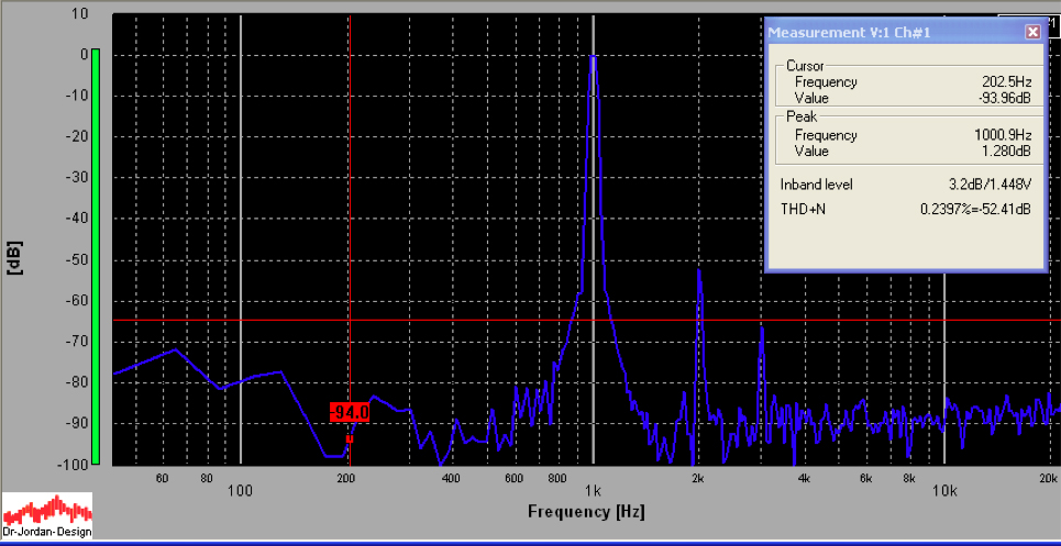
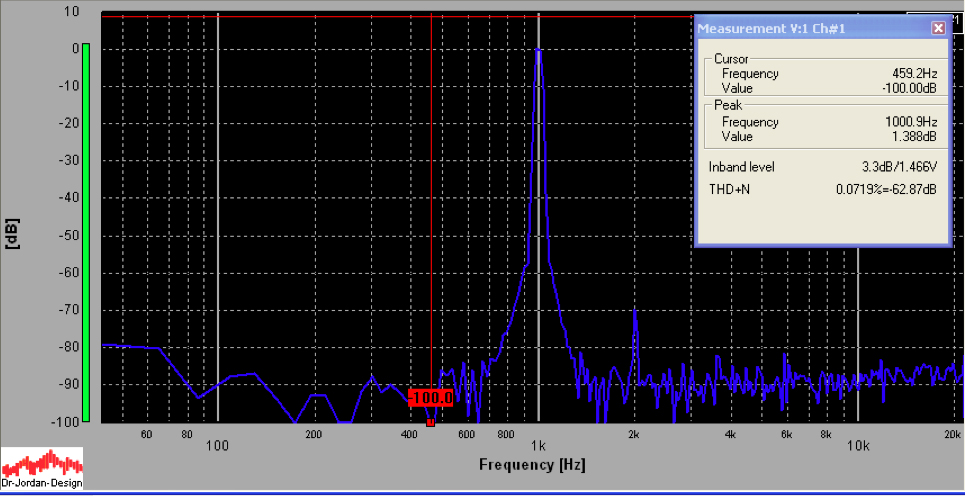
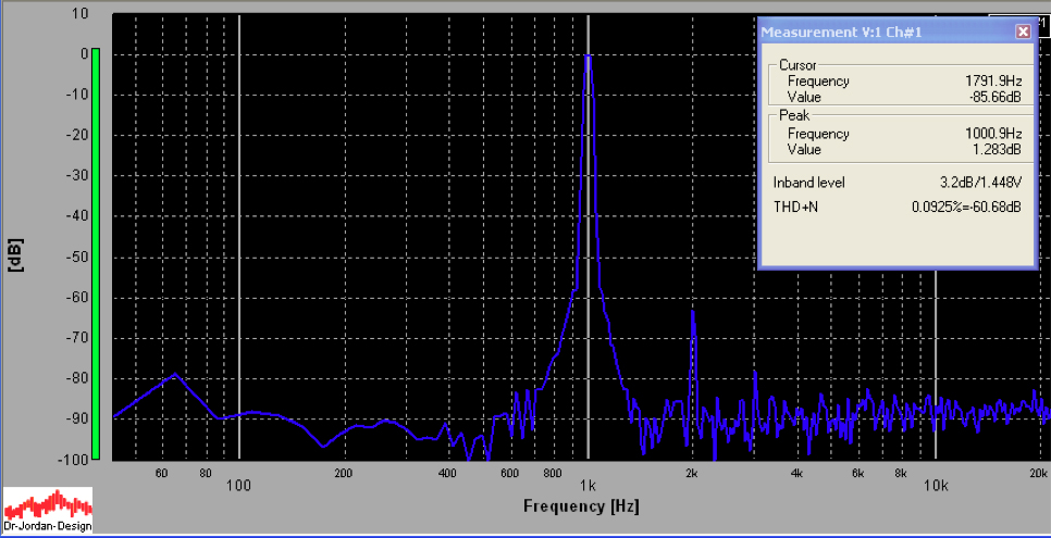
Amplifier testing was done with Dr Jordan's WinAudioMLS, which utilizes a very high quality external soundcard to conduct tests. The FFT (Fast Fourier Transform) is shown below for the left channel at 2W, using the 4 ohm tap, with no feedback. Note that even with no feedback, the distortion (THD+N) is a very respectable .24%. The noise floor is a respectable -90dB.
The FFT below is the same as the one above, but with 20dB feedback applied. Note the reduction of distortion to .07%.
12dB is shown below. The THD+N is only .09%.
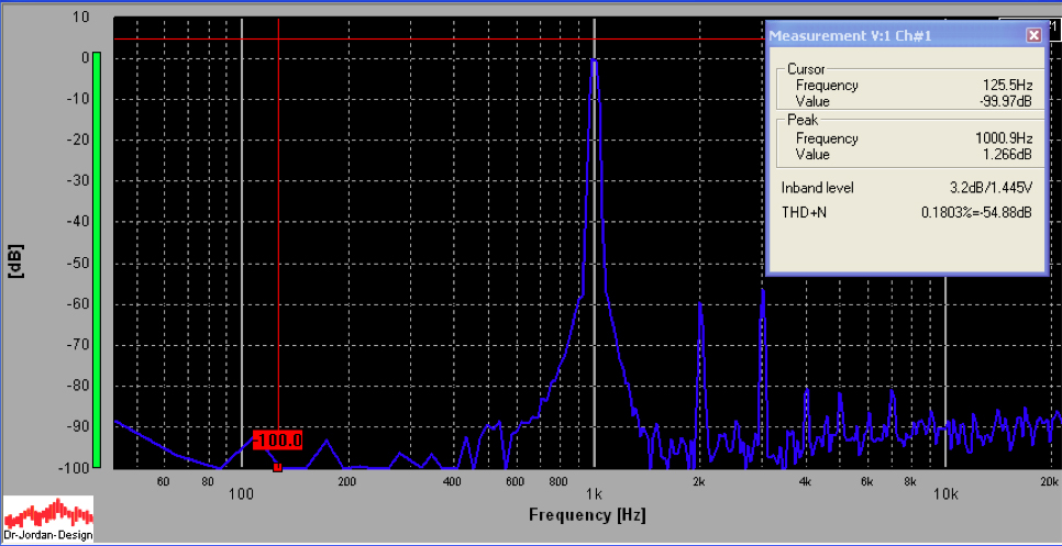
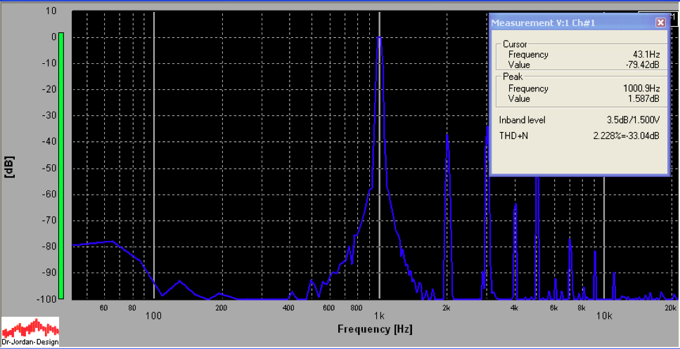
The power was cranked up to 50W, no feedback off the 8ohm tap. This is a brain-shattering volume. The resulting FFT is shown below. At full power, the distortion is not bad (2.2%).
This improves to .55% with 12dB of feedback.

...and to .18% with 20dB of feedback.