
BEN'S UNNECESSARILY COMPLICATED AMPLIFIER

1May2016
This is my 3rd push-pull amplifier, this time using the beefy 6550 power tubes (KT88's). It is switchable between ultralinear mode and triode mode with varying degrees of feedback.
I built a 6.3V regulator with the intent of regulating all voltages but it produced a LOT of heat. IN reality, with a push-pull amplifier, it is not really necessary to use regulated DC voltage, so I used the 6.3VAC, and wired it carefully to avoid 60Hz hum. A humbucker was also added to make the amp dead quiet. The bias voltage and the +500V to the anodes of power tubes are not regulated, although using "capacitor multipliers", the ripple is reduced to millivolts. It is known that the 115VAC line voltage varies during the day. For example, if the line voltage goes up 5%, the unregulated filament voltage goes up 5% to 6.6V and the power tube anode voltage goes to 525V, significantly increasing the current through the tubes. At the same time, however, the unregulated bias voltage becomes more negative, biasing the power tubes colder, thus offsetting this effect somewhat.
The previous amp had messy logic circuitry for soft-start, clunky controls and more messy logic circuits for bias voltages and cathode currents, with an analog ammeter, and frankly, not very good circuit protection in the event of overcurrents, etc. This new amp employs a microcontroller to control every facet of startup, circuit protection, and automatic shutdown by monitoring all voltages, as well as power tube cathode currents, temperature, and, in future projects, input and output from a preamp. More on this later.
Below is the amp opened up to show the interior viewed from the bottom. This was taken in March 2026, 10 years after it was completed. There is a tremendous amount of wiring outside of the printed circuit boards. The wiring for the tubes themselves is underneath all this. Everything is pretty well marked, and working on the amp has proven to be not a problem.

December2018. Ben reports that the amp is still working well, including the computer and screen.
14March2022. The amp went down recently after years of hard use. It seemed to be a power supply issue, so I started digging into it. The fuse was blown, so that was replaced, but on startup the transformer was loud - the core was clearly saturating. It was unclear exactly why. I pulled the circuit boards out and checked all the connections to the tube sockets. Sure enough, one of the grid leads was completely disconnected from the grid to one of the power tubes, and on another power tube, the tube socket was defective, so the grid only intermittently got the -50-60V it should have gotten. As a result, the tubes would periodically draw massive amounts of current. I replaced the defective tube socket, and reconnected the grid lead to the grid pin on the other socket. Several resistors had blackened as a result of the huge current spikes, so I tested and replaced components as needed.
Another issue was the crappy Chinese potentiometers I used to control the grid voltage. These were all replaced with American (expensive) potentiometers and should last a good long time.
Finally, the holes cut in the top plate of the amp chassis are really too small for the 6550 tubes, and the tubes were clearly damaged forcing them through the small holes. So, I decided to replace them with the thinner KT-90 tubes, which have the benefit of having a slightly smaller diameter, and so fit easily through the holes. They are also more powerful tubes and can be run at higher currents. Look on the "Less Complicated KT-90 Power Amp" page for the Power Stage calculations.
March2026. The power supply was humming loudly and the amp was not performing - almost certainly due to aging electrolytic capacitors in the power supply. Those were replaced with correction of the problem. One of the6SN7 driver tubes was failing, so it was replaced with restoration of the pleasant sound this amp has. I made some measurements and decided that I wanted to reduce the amount of feedback (see below).
While making measurements, the 6SL7 input tube decided to crap out after 10 years so it was replaced. Also, somehow or another I blew out the Teensyduino 3.5 microcontroller. No problem, I'll just spend $25 and replace it in its socket. But wait, they have stopped producing them and they are no longer available. Grrrrr! So, I had to design yet another board to hold the latest and greatest Teensyduino 4.1. This was done fairly easily and is shown below.
POWER STAGE
NOTE: the original amp used 6550 (KT88) tubes, but I made the decision in 2022 to convert to KT-90. The description below is identical to the description of the power stage for the Less Complicated KT90 Power Amp.
POWER STAGE
The characteristic curves for a KT-90 power tube, both Ultralinear and Triode mode, are shown below. The operating point will be at Va=500V and Ia = 60ma, for an idle dissipation of 30W, well under the maximum of 42W. The operating points are indicated by the red dots. Class A operation is shown by the blue line and corresponds to an Ra-a = 3.3K (1/2 of the transformer Ra-a of 6.6K.) Class A operation ends when Ia hits 120ma (2 X 60ma), because this means that Ia goes to zero when the sine wave goes maximally negative. Class AB operation is indicated by the purple line and ends when the grid voltage hits 0V (grid current begins to flow). The bias voltage, from the curves, is around -52V for ultralinear and -62V for triode.


POWER CALCULATIONS:
Class A1 operation (Ultralinear and Triode): P = .5 * Ia2 * Ra-a = .5 * .062 * 6300 = 11.3W
Class AB operation (Triode): P = [2*(500-140)/]2 / Ra-a = 39W
Class AB operation (Ultralinear): P = [2*(500-38)/]2 / Ra-a = 65W
So the amp can theoretically produce 65W in ultralinear, 39W in triode. In actual measurements, the amp doesn't get this nearly this much power before unacceptable distortion occurs. However, 50W should be attainable in ultralinear mode.
INPUT STAGE
We need to determine the amplification required from the input stages to drive the power tubes to full power.For the purpose of calculations assume a max Vi = 1.4V RMS (2V peak). With feedback, the actual voltage Vgk at the grid of the first stage is found with the following expression:
FB (in dB) = 20log(Vi/Vgk).
FB=6dB: Vi=1.4 => Vgk = .70Vrms
FB=12dB: Vi=1.4 => Vgk = .35Vrms
Note that there is about -50VDC applied to the grids of the KT-90'S by the biasing circuitry (see above curves - look at the red dot). So to get the power tubes to full power (Vgk = 0), you need about 50Vp (37Vrms) coming from the input stages.
So the amplification required from the input stages leading to the power grids is:
FB=6: A = 37/.7 = 53
FB=12:A = 35/.35 = 106
So, the input stages will need to be capable of providing a gain of at least 106 to push the power tubes to full power with maximum feedback in place. This should be very easy to attain. The 6SL7 has a gain of 60 alone.
Below are the characteristic curves for a 6SL7. A pretty linear looking area is around Ia=2ma and Vgk (Ef in graph) = -2V. This is indicated by the red dot. Vk is established by setting the cathode resistor equal to 1 kohm (1kohm * 2ma = 2V)
The cathode resistor is divided into a 953ohm resistor and a 47 ohm resistor. The top of the 47ohm resistor is the injection point for feedback.


This is just a grounded cathode amplifier with Ra replaced by a CCS. The CCS is adapted (well, stolen) from Morgan Jones' "Valve Amplifiers." The voltage across R12 is determined by V across the LED (around 1.8V) + Vbe of the PNP transistor (around -.6). So the voltage across R12 is 1.2V. The LED compensates for any temperature variations of Vbe.
The operating is set at plate current = 2ma. The plate current is the current across R12. The voltage across R12 is always 1.2V so the current across R12 = 1.2/R12. Setting R12 = 600 ohms then gives a plate current of 2ma. Voila. The actual value turns out to be 620, and that is what is in the actual circuit.
This CCS blocks any AC current (since the current NEVER changes from 2 ma). This means that for AC, the anode resistor is infinity (actually about 30-40 Mohm).
The gain of a bypassed common cathode amplifier is
A = mu * Ra/(Ra+RL)
where Ra = anode resistor, RL = load resistor.
As Ra approaches infinity (possible with the CCS), A approaches mu. The mu of a 6SL7 is about 70, so the gain of this stage should be around 70. In reality it measures out around 60.
DIFFERENTIAL AMPLIFIER
A long-tailed splitter generates two waveforms, each 180o out of phase with the other. These are fed into the push-pull power stage.

The very linear 6SN7's will be used for this stage. Their characteristic curves are shown below. They are most linear with Ia > 6ma, according to what I read, and my own testing.
Each tube will have an anode current of 8ma, so the constant current sink in the tail is adjusted to 16ma. The constant current sink works as follows:
Voltage drop across D5=.7V, across D2=6.2V, across Vbe (Q2)=.7V, so by Kirchoff's Law:
.7 + 6.2 - V(R7) - .7 = 0.
So V across R7 is ALWAYS 6.2V. We can set the current by adjusting R7. R7 is set to 390 ohms, which gives I = 6.2/390 = 16ma, which means 8ma flows through each tube.
Now, Va = 400 - 8ma*22K = 224V.
This operating point is shown below as a red dot.
R1 and R2 are actually 23.5K (2 47K's in parallel), so they each drop 23.5*8=188V, which means voltage at each anode is 212V. Gain is about 7.5 or so making a total gain of the input stage greater than 400 (60 * 7.5), which is close to twice what is necessary.

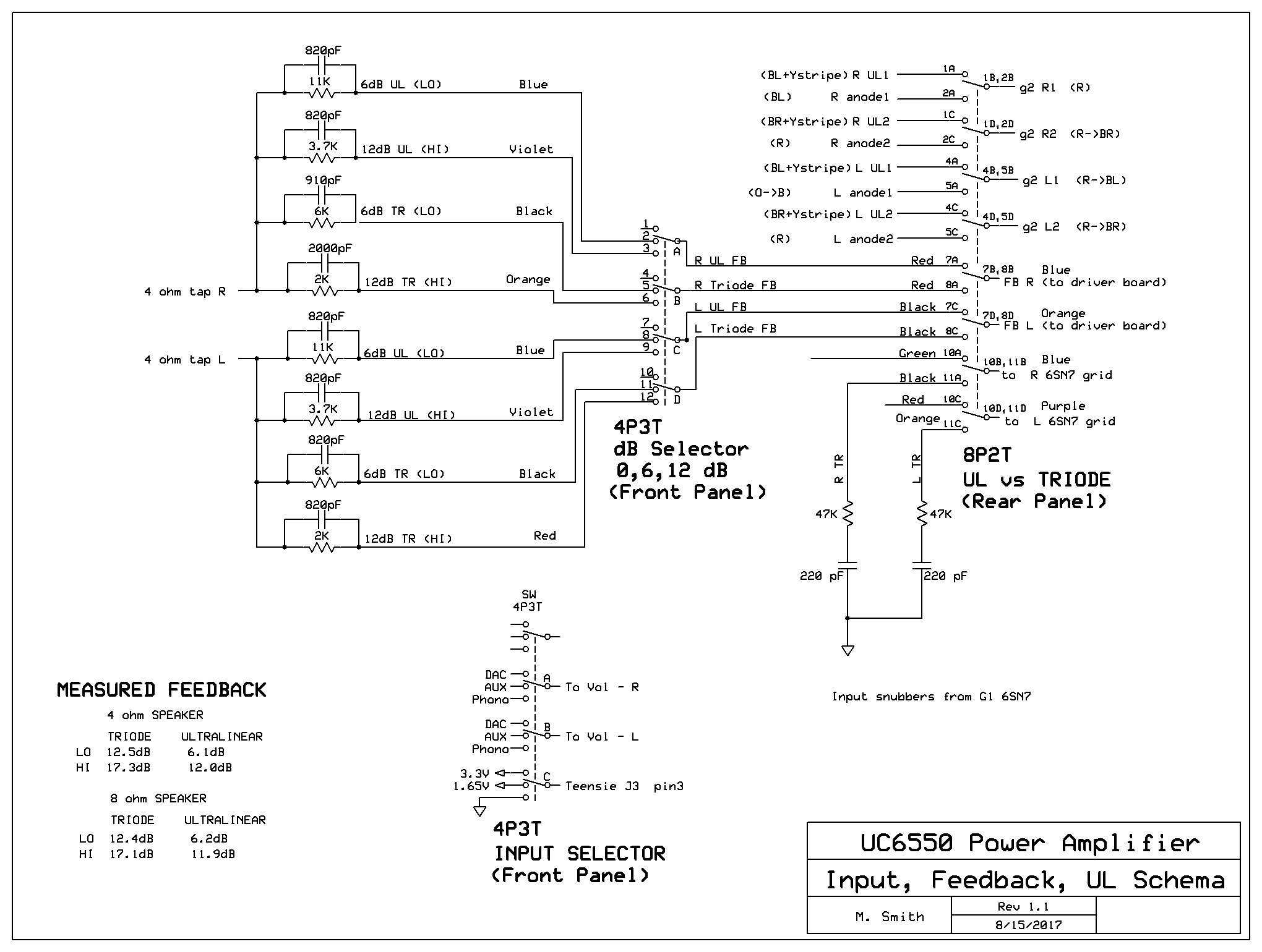
The PCB schematic for the drivers for both channels is shown below. Q5 and Q7 must be heatsinked. The feedback resistors with their capacitors are contained on a separate board and run through rotary switches to vary the amount of feedback..

The schema for feedback is shown below. A 3-position switch on the front panel controls the amount of global feedback (0,LO,HI) and a 2- position switch on the back switches between ultralinear and Triode mode. This is on the back because it can be dangerous for the health of the amp if this switch is turned with the amp on. Big warning label on the back. "LO" is 6dB for ultralinear mode and 12dB for triode. "HI" = 12dB for ultralinear mode and 17dB for triode. The values of the resistors were determined mathematically. I wrote an excel spreadsheet which does the calculations. The values of the capacitors were determined empirically as described below in the section on feedback compensation.
March2026. I decided to reduce the amount of feedback, so that now LO = 6dB for both UL and Triode, and HI = 12dB for both. This is reflected in the revised feedback scheme below.
BIAS CIRCUTRY

The power tubes will require about -53Vdc applied to each grid in ultralinear mode and around -60Vdc in triode mode. The bias circuit for each tube is shown here. These will be point-to-point wired so no PCB is necessary.
The bias for each power tube will be controllable from the front panel of the chassis by 4 10K potentiometers, shown as U1 in the schematic.
The bias controls the anode current as well as the screen current. With the pot rotated fully counterclockwise, bias voltage will be about -66V, and fully clockwise, -45V.
Cathode current, an OK proxy for anode current is measured across the 1-ohm cathode resistor.
THE MICROCONTROLLER

After messing around for a long time with an Arduino Uno microcontroller and actually designing circuit boards to attach to the arduino board, I concluded that it took up too much space. Note that the final board(s) has 3 levels to handle the multiplexer and shift register that are required because the Uno doesn't have enough I/O ports.
The arduino Uno board is the green one on bottom. The two above were designed by me.
So after a lot of work and a little money, I abandoned the Arduino Uno and looked for a more compact microcontroller with a lot more I/O pins.
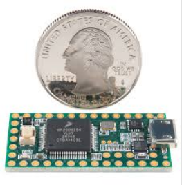
This little sucker is a teensy32 microcontroller. It has basically the full power of the Arduino Uno, but it has 21 digital I/O pins, 19 digital/analog pins, and 2 pins that are analog only. That is a total of 42 I/O pins! 22 of the pins are PWM. That is insane.
Absolutely no need for a multiplexer or shift register or any of the other cumbersome logic required by the Uno.
Update May2021. The amp was acting up, mainly due to the crappy plastic power connectors used to connect the power supply to the amp. In the process of upgrading those, I guess I fried the Teensy 3.2 microcontroller. Unfortunately, the way it is designed, it cannot be plugged into an IC socket, but must be soldered directly to the board. So, the whole board needs to be replaced.
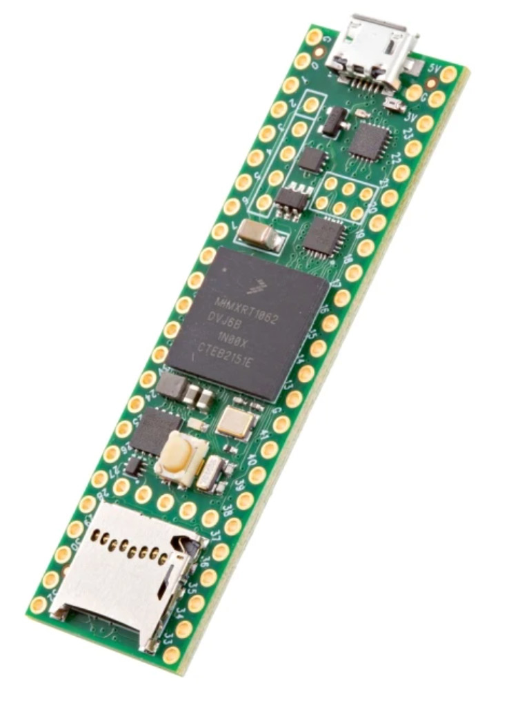
So, I designed a new board around the Teensy 3.5, which is bigger than the 3.2, but it has plenty of pins on its top side so I don't need to use any of the pins on the bottom, so I can plug it into a 48-pin IC socket, and just pop it out and replace it if I ever fry it again.
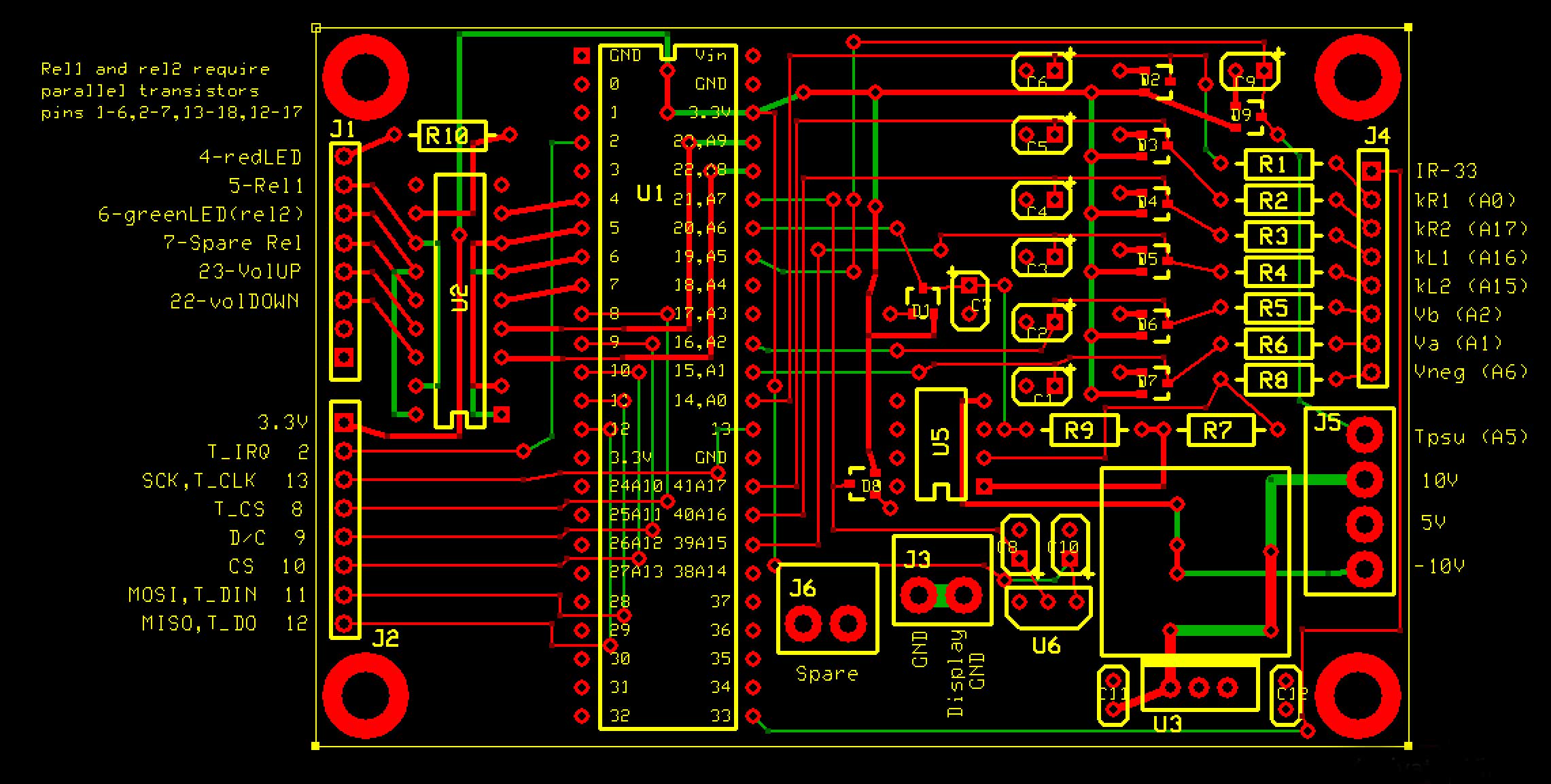
Update April2026. Well, I did fry it, but replacements are unavailable, as stated above. So, I had to design a new board around the Teensy4.1, which wasn't that big of a deal, but cost me $135 for fabrication and absurd rate for shipping.
The new design is shown below. There is only one LM358 op-amp to convert the negative Vneg voltage to positive. All the analog inputs are voltage protected by a Schottky diode keeping voltage below 3V and a second Schottky to keep it above 0V. These are contained in a BAT54S SMD package. I got rid of the negative voltage regulator and just ran -10V unregulated into the op amp.
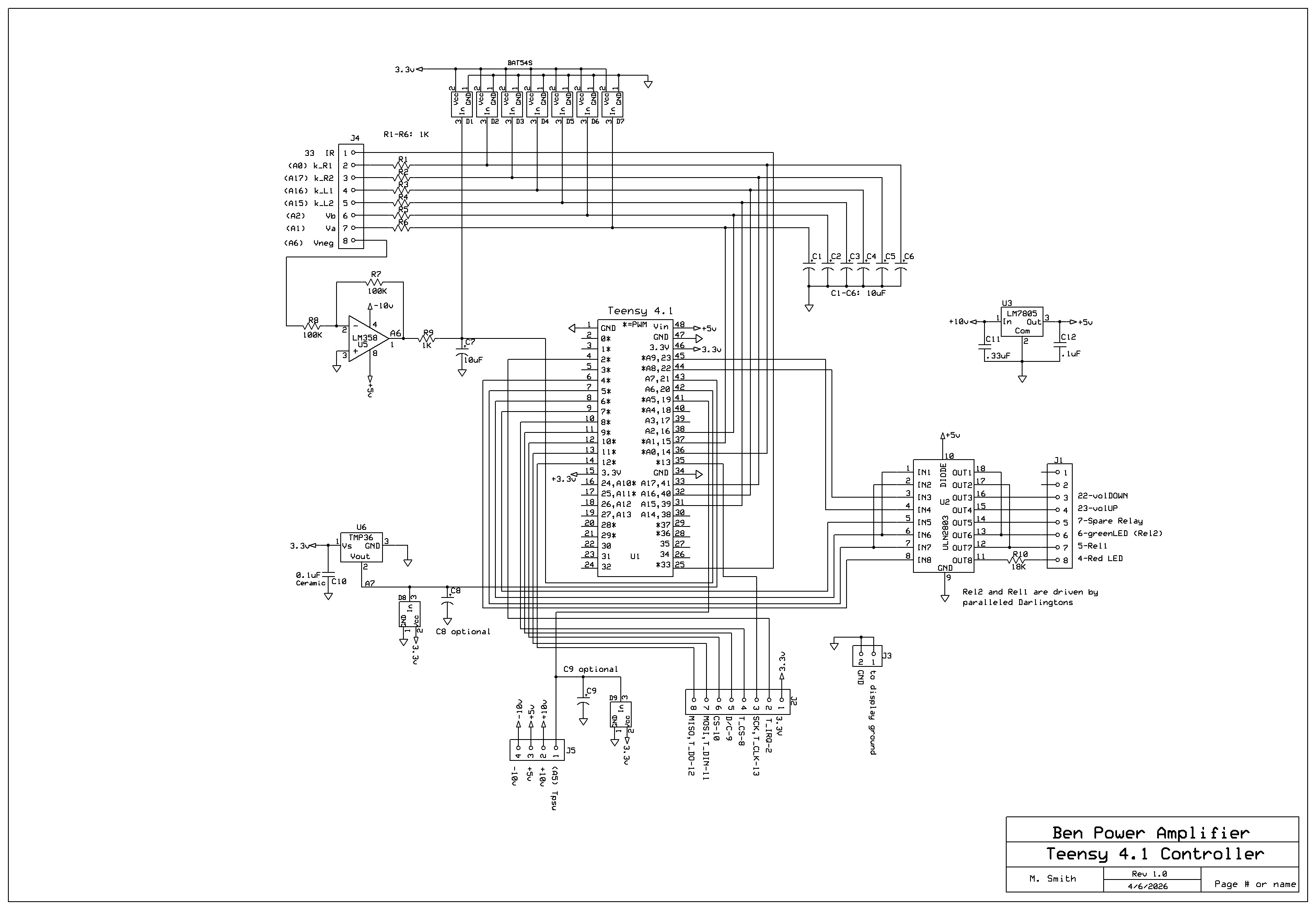
Below is the design of the PCB to be sent for fabrication. Note the position of U6, the PSU temperature sensor located literally almost touching the heat sink for the 5V regulator. Not smart. I mounted the sensor on the bottom side of the board, hopefully far enough away from the heat sink.
Some of the inputs from the amp are 400-500V. I really don't want these voltages coming on to my delicate little teensy3.5 board, so the little circuits to the left reduce these voltages to appropriate levels for inputting into the teensy. The Teensy inputs are protected by the BAT54S's described above.
Output impedances of these little dividers are around 1K which is perfectly fine for inputting into teensy.
Corrections will be made in the Arduino program.
POWER SUPPLY
The power supply consists of the transformers and rectification sitting in its own chassis plus a voltage regulator and smoothing circuitry sitting in the amplifier chassis. The power supply chassis is connected to the amplifer chassis by a 12-conductor power cable. Below is the schematic for the circuitry in the power supply chassis.

After rectification, 560V and -100V are sent to the amplifier chassis to be conditioned further. A 12V supply is also sent, as well as the 6.3V AC for the tube heaters.
A note about the relays. These are controlled by the Teensy microcontroller in the amplifier chassis, and are used to provide a slow start for the big transformer.
When the transformer is powered on and rectified, huge currents flow into the capacitors until they are charged. This can actually cause the house lights to dim. To mitigate this somewhat, Relay 1 is energized first, which means the current going into the transformer is limited by the 25W 12 ohm resistor. After a period of 150 milliseconds, relay 1 shuts off and relay 2 is energized which allow full current to flow into the transformer. Red and Green LED's show the progress of this startup.
COMPENSATION NETWORK
Below are the square responses of the UC6550 with feedback in both triode and ultralinear modes. There is significant ringing in all modes except ultralinear with 6dB. This means that the amplifier could be unstable at high frequencies without compensation networks put in. All compensation networks are designed to attenuate gain at high frequencies.


Below is the entire amp with the compensation networks circled. The method I used was taken from a great article by Tim E. Smith on angelfire.com entitled "Empirical implementation of global negative feedback."
The first compensation network is at the output transformer. The technique is taken from Radiotron Designer's Handbook, 4th edition from the 50's. It recommended a resistor value equal to the Ra-a of the transformer. So 6.8K was close enough. C = 1/(100000*Ra-a) = 1.5nF.
The next snubber is at the input to the differential amplifier. The values for R and C are derived entirely empirically. I adjusted a 100K potentiometer and a variable capacitor to eliminate the ringing with the least amount of high frequency attenuation. It turns out that in the ultralinear setting, no input snubber was really necessary. The optimum values that seemed to work with the triode setting at both low and high feedback settings were R=10K and C=220pF.
Finally, a capacitor is placed across the feedback resistor itself. Remember that the feedback resistor shown is actually a choice of 4 resistors per channel, selectable by the mode switches as shown above on the "Input, Feedback, UL Schema" diagram. The capacitor for each resistor is adjusted until the desired effect is achieved. The idea here is to reduce the reactance of the feedback network at high frequencies, thereby increasing the feedback and reducing gain.

The results of the adjustments are shown below. These are for triode mode with 17dB of feedback. I will only show the right channel, because the left channel is essentially identical. A very nice square wave is seen with the 1kHz square wave input. No ringing or raggedness. At 3kHz it's not quite as crisp, indicating that there is some high-frequency rolloff. At 10kHz, there is some definite rounding on the leading edge. Only a very small percentage of people can hear 10kHz anyway, and definitely nobody of my advanced age. I happen to hate the harsh sound of some amplifiers, and I think that the compensation networks as designed give a very slight treble reduction which I find desirable. So far, nobody has said that there seems to be something missing at the high frequencies in my amps.


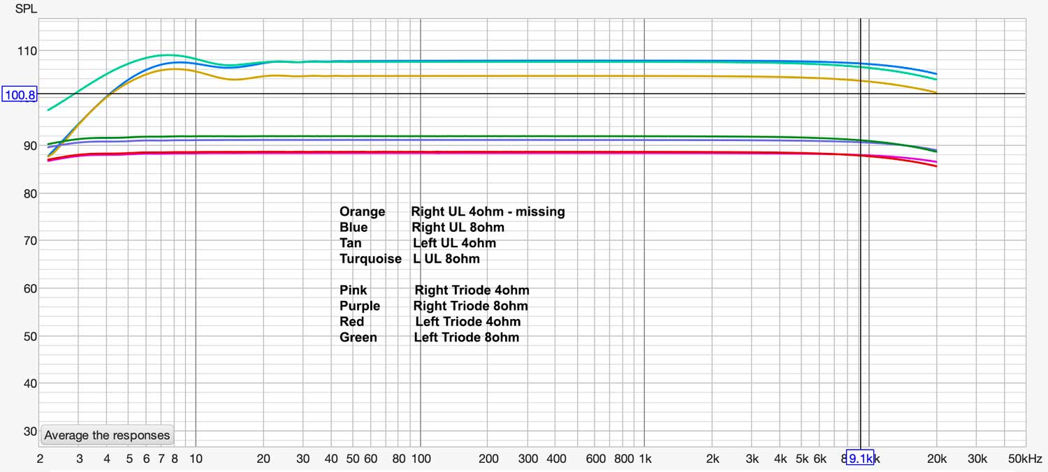
Frequency Response
The frequency response curves are shown below. The top set are ultralinear mode and bottom set are triode. Pretty flat out to 10kHz with only a 1-2dB drop at 20kHz. Good enough.
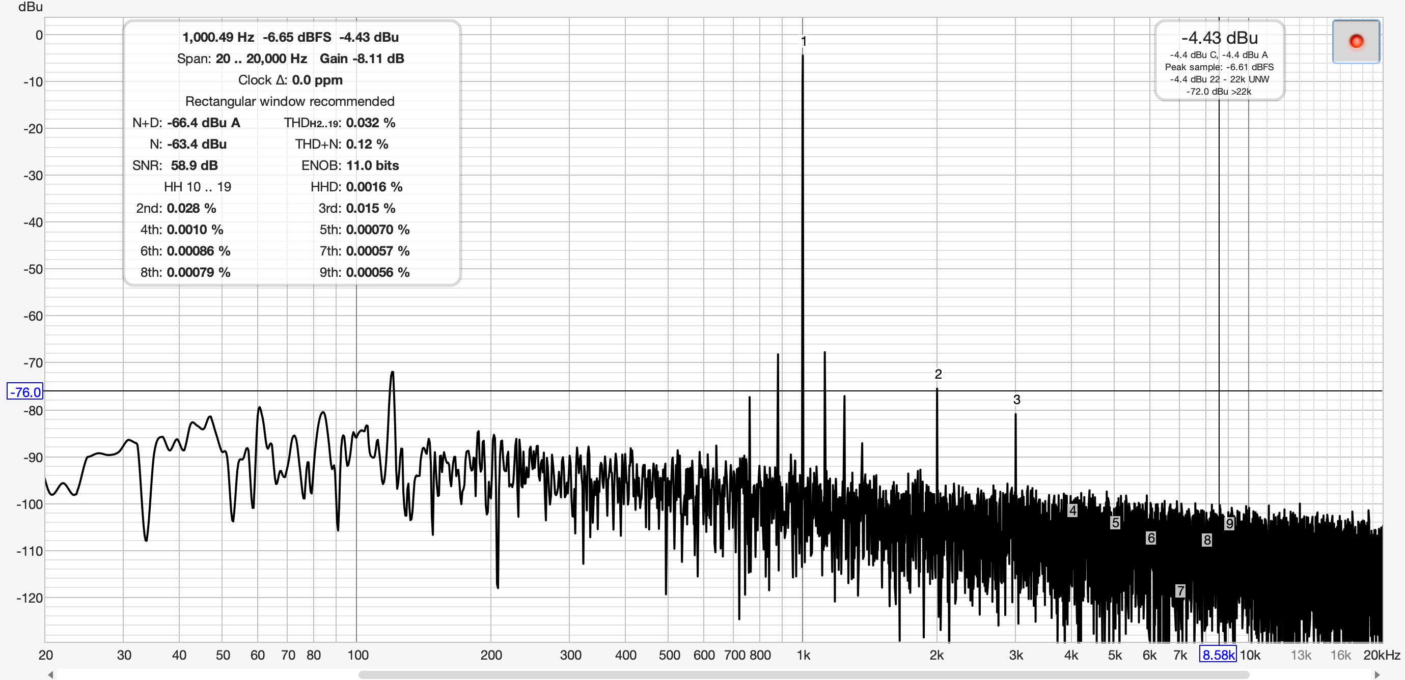
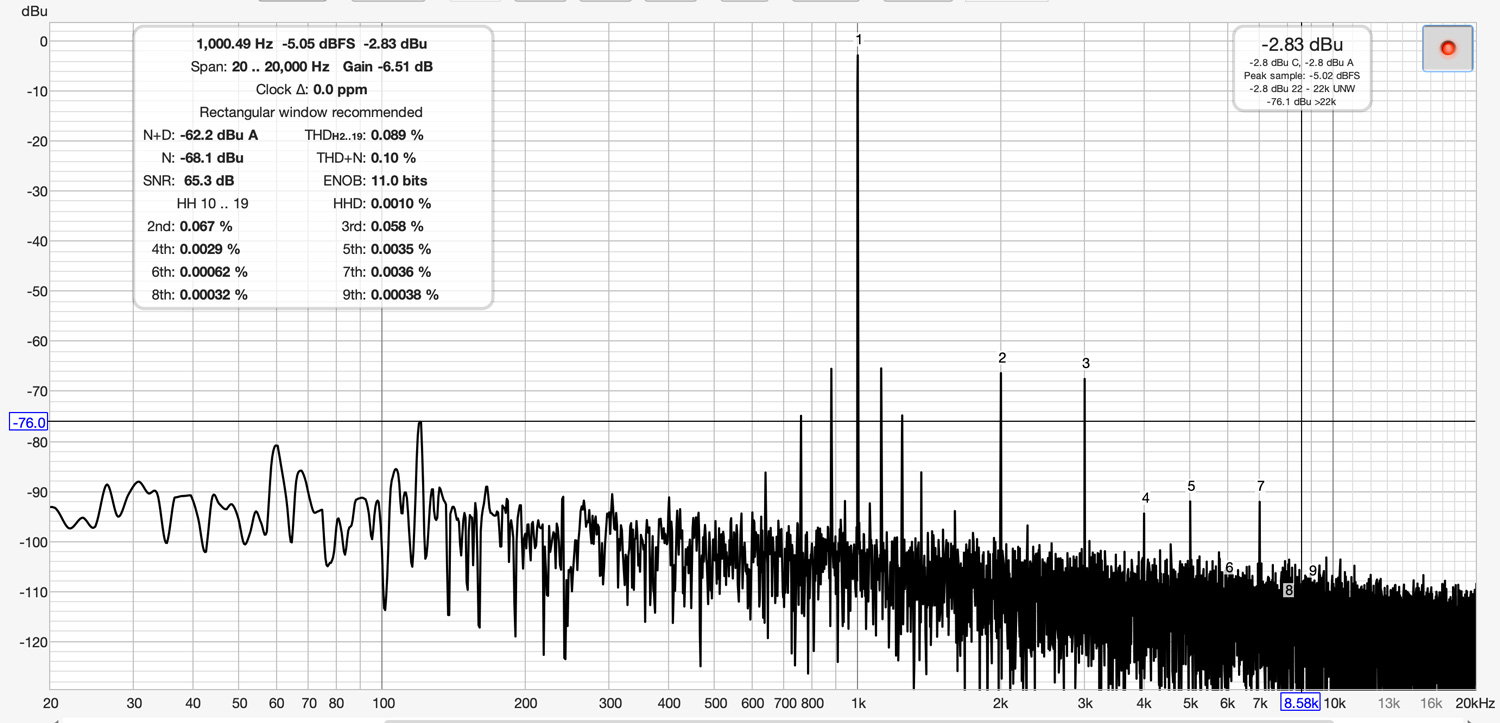
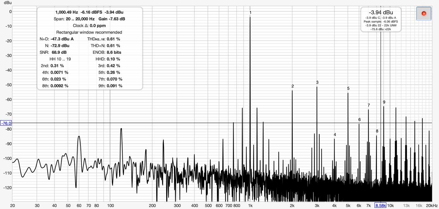
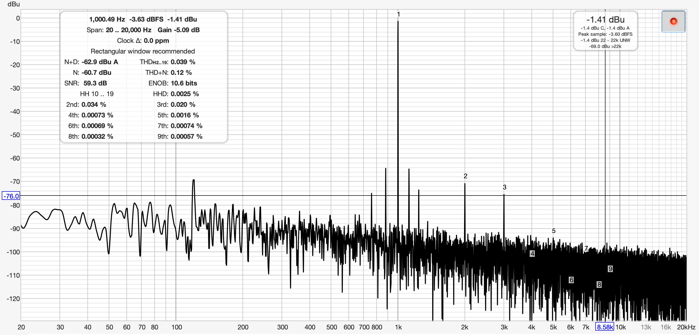
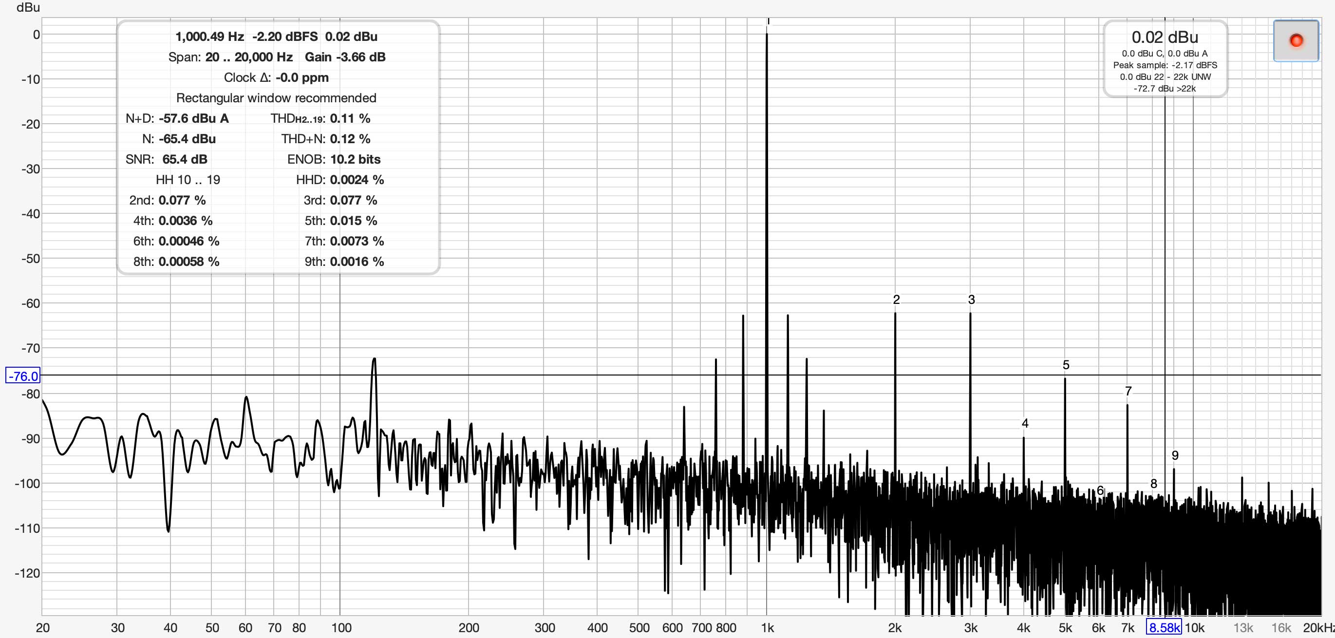
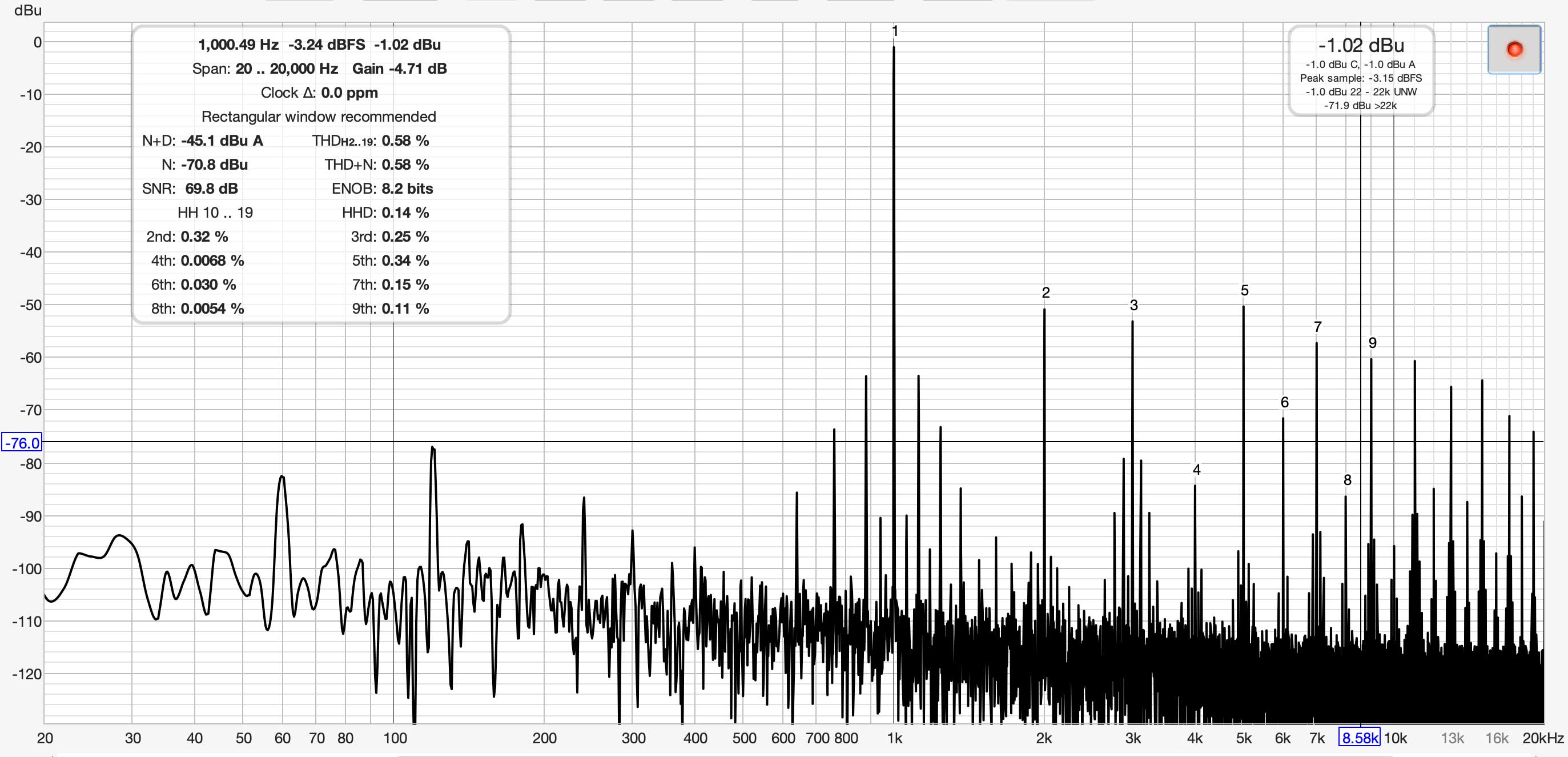
DISTORTION MEASUREMENTS
All distortion measurements were made with feedback set to HI (12dB). The FFT's (fast fourier transforms) are shown below for both triode and ultralinear settings. Only the left channel is shown. There was no difference between left and right channels. Note the extremely low distortion all the way out t0 60W, near clipping. I'm not loving the peak at 120Hz, from the power supply rectification, but I can't really hear it coming from the speakers, so I won't worry about it.
Left Ultralinear 4ohm 1W
Left Ultralinear 4ohm 5W
Left Ultralinear 4ohm 60W
Left Ultralinear 8ohm 1W
Left Ultralinear 8ohm 5W
Left Ultralinear 8ohm 60W
Left Triode 4ohm 1W
Left Triode 4ohm 5W
Left Triode 4ohm 60W
Left Triode 8ohm 1W
Left Triode 8ohm 5W
Left Triode 8ohm 60W