HOT-1 TUBE-BASED PHONO PREAMPLIFIER
12January2019
I decided to resurrect my old beautiful Denon Turntable, even replacing the aging phono cartridge. My JFET based NAD phono preamp worked OK, but there was too much irritating noise, so I decided to look into building a tube based preamp that is dead quiet, hopefully built with Hopelessly Outdated Technology (HOT). My research took me to a very interesting article at diyaudio.com entitled "His Master's Noise: A Thoroughly Modern Tube Phono Preamp." The article is by an interesting gentleman named Stuart Yaniger who goes by the moniker SY. The article can be found here. Most of the amp is based on this article.
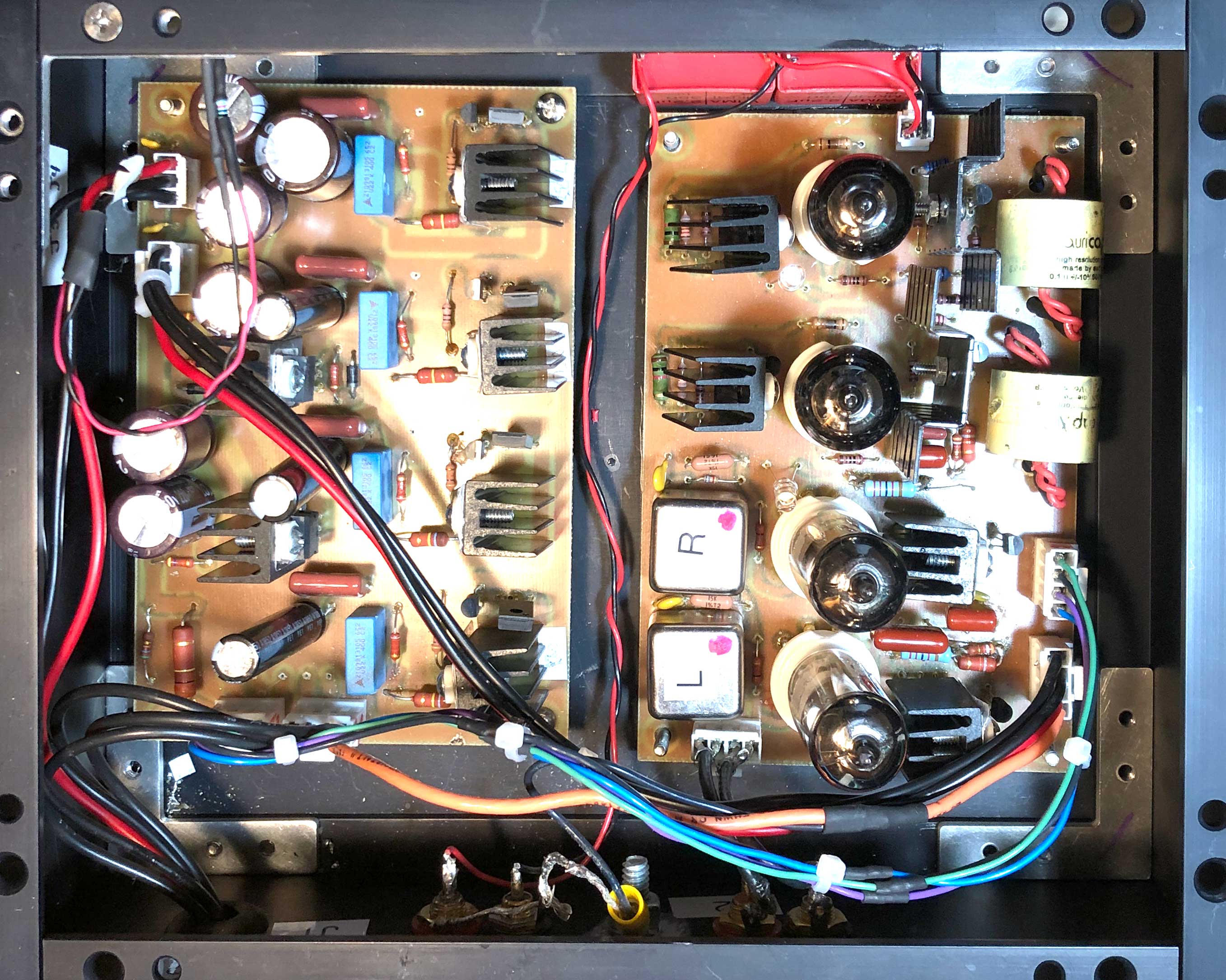
Below is the guts of the completed amp. The separate power supply is not shown. The entire circuit is contained on 2 DIY circuit boards, designed and built by yours truly. They are a little rough, but seem to work fine.
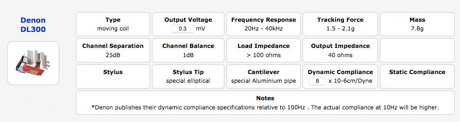
The specs for my phono cartridge are shown below. The first problem to pop up is the output voltage of this cartridge - it is a tiny little 0.3mV. This is going to take a lot of amplification to get it to the .5-1V needed at the output of the preamp. And any noise that finds its way into the system will be amplified hugely too.
The first thing to do is to calculate the unavoidable noise contribution of the cartridge itself. The noise produced by a device (like a resistor) is given by the following equation. Richard Feynman apparently derived this from scratch in his "Lectures on Physics."
Vn = √4KTRΔf
where K=Boltzmann's constant, T is the temp in degrees Kelvin, R is the resistance, and Δf is the bandwidth (20-20,000Hz for audio).
Using the output impedance of 40 ohms as R, and room temperature for T, you get Vn = 192nV.
Since the output signal is .3mV, this gives a S/N ratio of 64dB. The designed circuit should strive to be better than that.
TOPOLOGY
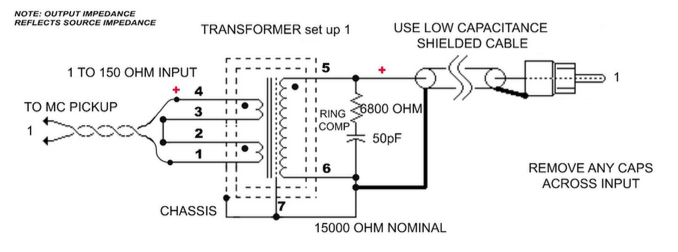
I bought off Ebay some Jensen transformers designed to be used for MC phono cartridges. They are configurable to step-up either 1:10 or 1:20. I will use them as 1:10 step-up transformers as shown below. The 6800R resistor and the 50pF capacitor are there to reduce ringing, I think. The advantage to transformers is that they allow for a balanced input which will reduce noise.
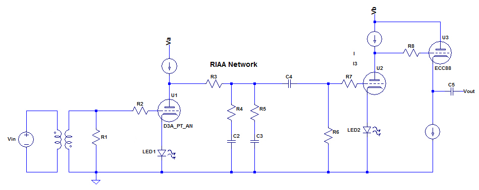
So, the transformer steps up the .3mV signal to a 3mV signal. The next stage is a gain stage, followed by the passive RIAA network described below, followed by another gain stage, and then a cathode follower to drive the cables leading to the power amplifier. The whole thing is shown below, greatly simplified. Note the extensive use of constant current sources and sinks and LED's for biasing. There will be a lot of silicon in this tube design, but I am not a purist. I don't even like purists.
The load impedance seen by the cartridge (shown here as Vin) is determined by R1 (above schematic) as it is reflected through the transformer. Since this is a 1:10 transformer, the impedance seen by the cartridge is R1/102 or R1/100. Now, according to the cartridge specs above, the load impedance has to be greater than 100, so R1 has to be greater than 10K to make the cartridge happy. This shouldn't be a problem. I'll start with a 15K resistor for R1. This transforms through the transformer to 150R, which is the load impedance the cartridge will look at. If the square wave response is fine, I'll leave it at that. Note that this cuts down the paltry cartridge voltage from .3mv to
[.3 * 150/(150+40)] = .24mv .
ATTENUATOR
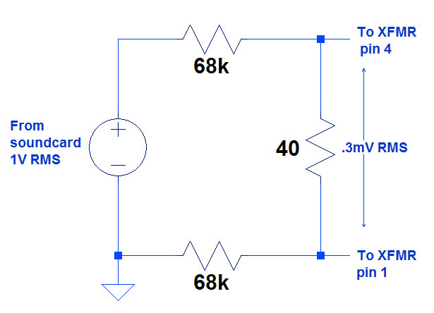
To do testing on this amp, it is necessary to simulate the cartridge with a
voltage source of .3mV and 40R output impedance. The attenuator to the
left does this. The voltage source on the left is the input from my test
soundcard. The output is taken off the 2 ends of the 40R resistor.
Vo = 1 * 40/(136K + 40) = .3mV RMS
Rout = 40R in parallel with 136K ~ 40R
FIRST STAGE
The first stage should provide as much amplification as possible but should also have a low output impedance. The reason for this will be explained later. Suffice it to say that you should try to keep output impedance (Rout) as low as possible.
Now, for a common cathode amplifier like the first stage:
Rout = ra ∥ Ra
where Ra = external anode resistor, and ra = the anode resistance, found in the tube datasheet.
I am using a CCS (constant current source) as the anode resistor in the first stage, and this represents a AC resistance in the 10's of Megaohms, or basically infinity. So the output impedance Ro = ra. So we are looking for a tube with as low an ra as possible. We'd also like a high mu tube to maximize amplification. Since
mu = ra * gm
this means a high gm (transconductance) tube. All modern phono preamps use high tranconductance tubes, and as a result, the really good high-transconductance tubes have become stupidly expensive, some costing $500 or more apiece. The best alternative is the D3A pentode strapped in triode mode, as recommended by Mr. Yaniger. When he recommended it, the cost was around $10 a tube. Now that it has been discovered it is around $100/tube. It has a transconductance (gm) of around 35, a mu > 70, and a plate resistance of less than 2K, so Rout should be less than 2K. I managed to find a Russian guy on Ebay selling D3A's for about 60 bucks per pair, so I bought a couple.
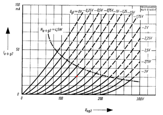
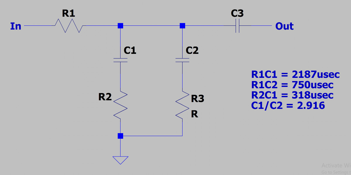
The published characteristic curves for the D3A in triode mode (from the 1950's LOL) are shown below. A common operating point is indicated by the red dot. 20ma anode current, 140V at the anode and Vgk = -1.25V.
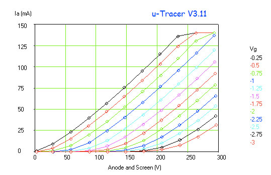
I measured the tubes using my kit-built uTracer3. Click here to see a little blurb on this awesome piece of engineering. The measured characteristic curves for tube A are shown below. These compare pretty favorably with the curves published 60+ years ago.
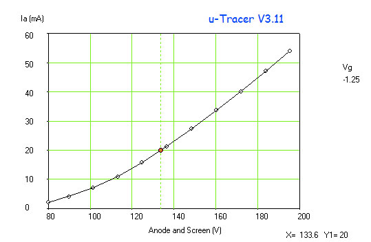
I'll stick with the operating point at Vg = -1.25V. The single curve for that grid voltage is shown below. The operating point of Vg=-1.25V and Ia=20ma is indicated by the red dot. You can see that the expected voltage on the anode should be 133.6V
Now, ra, the intrinsic anode resistance of the tube, mentioned above, is:
ra = dVa/dIa
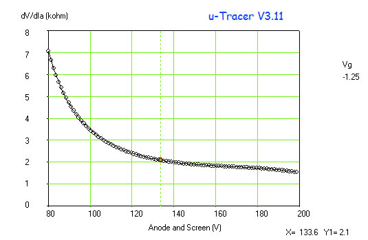
Yes, this is the derivative from calculus. The genius who developed the μTracer figured out a way to differentiate this curve, by estimating it with a 3rd, 4th, or 5th order polynomial, whichever is closer. The plot of dVa/dIa is shown below. At the operating point, ra = 2.1kohm. Voila
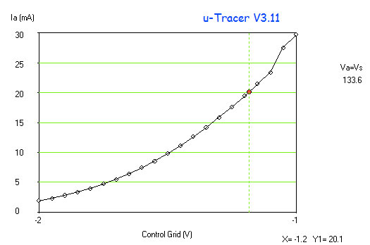
The μTracer will also plot Ia vs Vg curve. I plotted a single curve with Va = 133.6V. It is shown below.
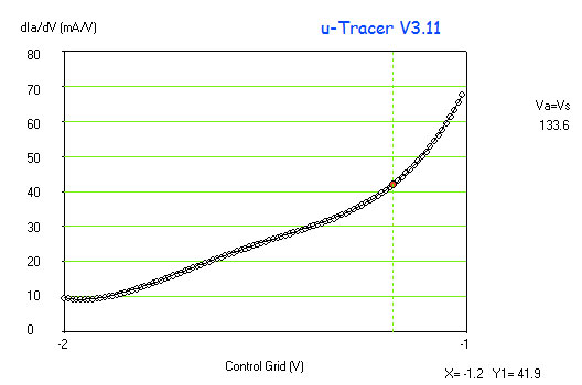
More elementary calculus: the transconductance gm is the derivative of the I vs Vg curve shown above. The μTracer will plot the derivative of the curve also and it is shown below: Note that at the operating point of Vg = -1.2V (close enough), the transconductance is 41.9. Awesome!
Since mu = gm * ra, we can predict that
mu = 41.9 * 2.1 = 88. Thus, we can expect a gain of around 88 from this tube. Pretty good.
Repeating this whole exercise with tube B gave the following results:
ra = 2.3kohm
gm = 37
mu = 85
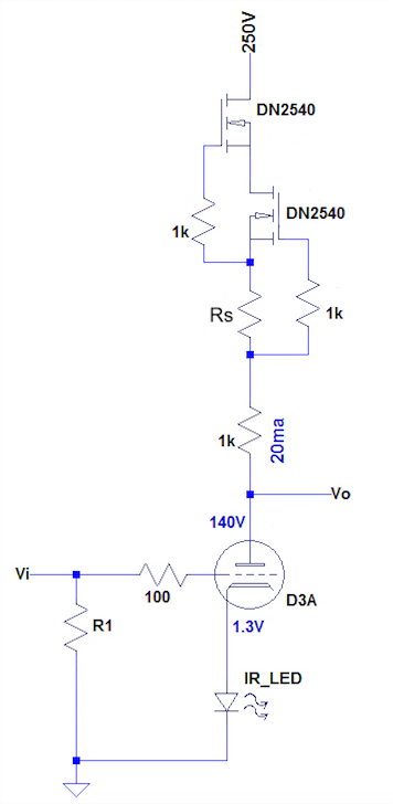
The first stage is a simple common cathode amplifier. The MOSFET cascode on top is a basic constant current source (CCS), made up of depletion-mode MOSFETS. The current is set to 20ma by Rs. The advantages of a CCS as the anode load for a common cathode stage are many. Because the current is dead constant at 20ma, any changes in voltage at the anode of U1 will not cause a current change through the CCS, i.e. the CCS represents almost infinite resistance to AC. This means lower distortion, and the maximum gain possible from the tube.
For a common cathode amplifier,
gain A = mu * Ra / (Ra + ra)
where ra = intrinsic plate resistance of tube, and Ra = the anode load.
As Ra approaches infinity, A = mu. So we can expect a gain A of around 85-88 as found by measurement above.
Another advantage of a CCS is superior power supply noise rejection.
The cathode voltage is set by the infrared LES at 1.2V. This means that Vgk = -1.2V
The 100R resistor is a grid stopper to keep this high-transconductance tube from oscillating wildly. Hopefully that is enough. R1 is 15K and reflects back through the 1:10 transformer to present a 150R load to the cartridge.
Measurements of the first stage were done and showed the following:
Left:
A = 85
Rout = 2.3K
Right:
A = 88
Rout = 1.7K
RIAA COMPENSATION
RIAA equalization is a form of pre-emphasis on recording and de-emphasis on playback, established by the Recording Industry Association of America (RIAA). Hiss and other high-frequency crap is an annoyance of vinyl recording, but is pretty constant volume regardless of the recording volume. So the RIAA compensation records the high-frequency stuff louder, and on playback, the high-frequency stuff is de-emphasized (played softer) by the amp, thereby reducing hiss.
Another annoyance of vinyl recording is the fact that low-frequency sound requires a greater excursion of the stylus in the groove, necessitating wider grooves and greatly reducing vinyl real estate. The work-around is to de-emphasize the low frequencies on recording, reducing groove width, and emphasize the low-frequencies on playback.
This is shown below in the official RIAA equalization curve.
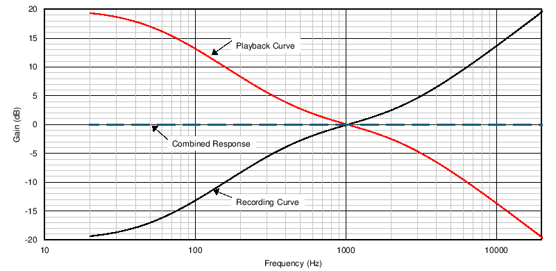
The recording companies do a good job getting the RIAA recording curve right. The following equation in the Laplace domain describes the recording.
Gain = (1 + 3.18-3 · s)(1 + 7.5-5 · s) / (1 + 3.18-4 · s )
Our job is to build a filter circuit to produce a playback curve that exactly counteracts the RIAA recording curves and produces the nice flat Combined Response curve. This is not a simple low-pass filter. It defines transition points in three places: 75 µs, 318 µs and 3180 µs, which correspond to 2122 Hz, 500 Hz and 50 Hz (rounded values). Mathematically, the pre-emphasis transfer function is expressed as follows, where T1= 75µs, T2=318 µs, T3=3180µs. Note that this equation is in the Laplace domain where s = jw = j2πf.
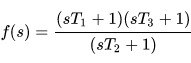
This can be approximated with many circuits, both passive and active. I will use the simplest passive circuit, because it works fine. It is shown below. Doing the calculations is staightforward. I wrote a little Excel spreadsheet that does them.
Remember that R1 is actually a composite impedance taking into account the impedance (Rout) of the first stage and the selected value of the resistor, so once we settle on a value of R1, we must reduce the actual resistor size by the value of Rout. Note that R3 is not included in these calculations. It will be discussed later.
Note that the components of this circuit are taking the full 140V DC from the first stage. The coupling capacitor C3 is placed after the equalization network so that it doesn't interfere in the RIAA circuit's function.
Using my handy-dandy Excel spreadsheet, I calculated that using C1 = 100nF gives R1 = 21.87K, R2 = 3.18K, and.
Now, remember R3 = Rout + chosen resistor. So I'll use a 20K resistor and trim appropriately.
I used a C1 measured at exactly 100nF. C2 was made up of a 33nF cap in parallel with a 1.5nf cap. R2 was 3.9K paralleled with 18K.
I made the following measurements with the voltage at 1000Hz as the reference voltage.
| Right | Left | |
| 20Hz | +19.5dB | +19.2dB |
| 50Hz | +17.0dB | +17.1dB |
| 1kHz | 0dB | 0dB |
| 2kHz | -2.7dB | -2.5dB |
| 5kHz | -8.4dB | -8.3dB |
| 10kHz | -13.1dB | -14.0dB |
| 20kHz | -21dB | -21dB |
I think that is close enough.
SECOND GAIN STAGE WITH CATHODE FOLLOWER
The original .3mV signal has been amplified X10 by the transformer, then another 73X by the first stage, giving a signal of 219mV.
By design, the RIAA network knocks a 1kHz signal down by 20dB (10X). So our 219mV 1kHz signal is knocked down to about 22mV by the RIAA network.
So, in order to get an output from the preamp of .5V (which is good enough for most power amps,) the second stage needs a gain of at least .5V / 22mV = 23.
A popular tube used in phono preamps and especially in cathode followers is the ECC88. It is very linear, especially when loaded with a CCS. It is low-noise. There are two triodes in a package, so one can be used as the second amplifying stage and its twin as the cathode follower. This is the tube SY used in his design, and it is the one I will use.
SY has a great deal of experience with this tube and he says that a particularly linear operating point is with an anode current of 10ma and Vgk = -1.7V. I simulated his circuit in LTspice and found a surprising amount of distortion, particularly 3rd harmonic. I decided to use the operating point recommended by Philips in their 1955 datasheet. It recommends Vak = 90V, Ia = 15ma, and Vgk = -1.3V. The characteristic curves for the ECC88 are shown below. To my eye, the recommended operating point (indicated by red dot) appears to sit in a more linear region, but that could just be my imagination.
The resulting circuit is shown below.
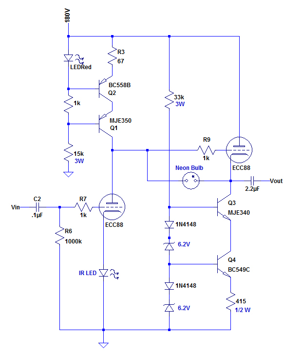
The gain stage is another common cathode stage with a CCS sitting on the
anode. The 15ma current is set by the 67R resistor and Vk is set at 1.25V
by the IR LED. Va-K comes in at about 89V. The gain is about 32.5.
The cathode follower has a current sink on its cathode, also set at 15ma.
The grid is pegged to 89.3V by the anode voltage of the gain stage.
And the anode Va = 180V.
This tube has no choice but to set its cathode at 90.6V giving Vak = 89.4V
and Vgk = -1.3V, which is exactly what is recommended by Philips.
The gain of the cathode follower, as expected, is .98.
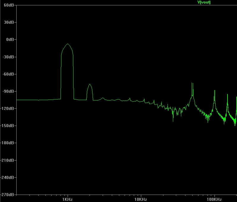
LTspice generated the following FFT (fast fourier transform) of the 2nd stage and cathode follower output. Distortion is low and almost exclusively 2nd harmonic. I think I will stay with these settings for the ECC88's.
Gain Measurements. Using a 1V RMS input, into the attenuator, I got almost exactly 2mV RMS coming out of the left and right transformers.
After the first gain stage, I measured 114mV on the right and 118mV on the left, making the gains of the first stages AR = 57, and AL = 59. The gains of the second stage/cathode follower were measured at AR = 63.5 and AL = 65.3.
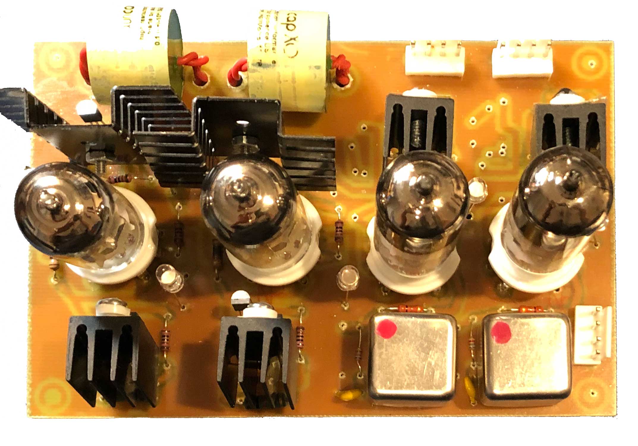
Below is the completed homemade amplifier board. The input transformers are the silver boxes with the red dots, and the output capacitors are the big yellow cylinders at the top. The D3A tubes are the two on the right, and the ECC88's are the 2 on the left.
RAW VOLTAGE POWER SUPPLY
The Raw Voltage PSU is housed in a separate homemade chassis. In order to have regulated 250V and 180V rails, the raw PSU should put out about 300-320V unregulated and 230-250V unregulated, both rails going to the main amplifier chassis to be regulated. In addition, to allow for 6.3V regulated filament supplies, the raw supply should put out about 15V unregulated voltage to go to the 6.3V regulators in the main chassis.
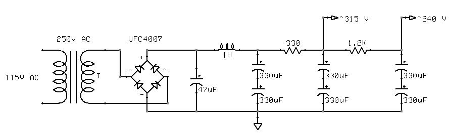
The raw unregulated rail voltages are produced by the simple stage shown below.
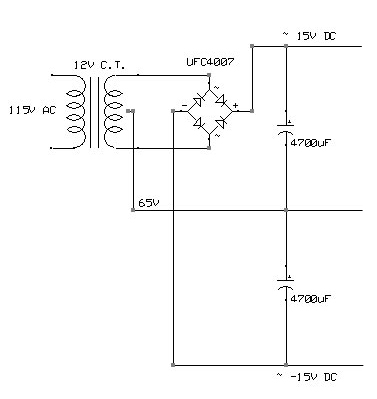
The unregulated +/- 15V raw supply is shown here. Note that the center tap is at 65V; this elevates the filaments, so that the cathode-filament voltage on the ECC88's is not excessive, as explained below. The 65V is brought from the amplifier chassis.
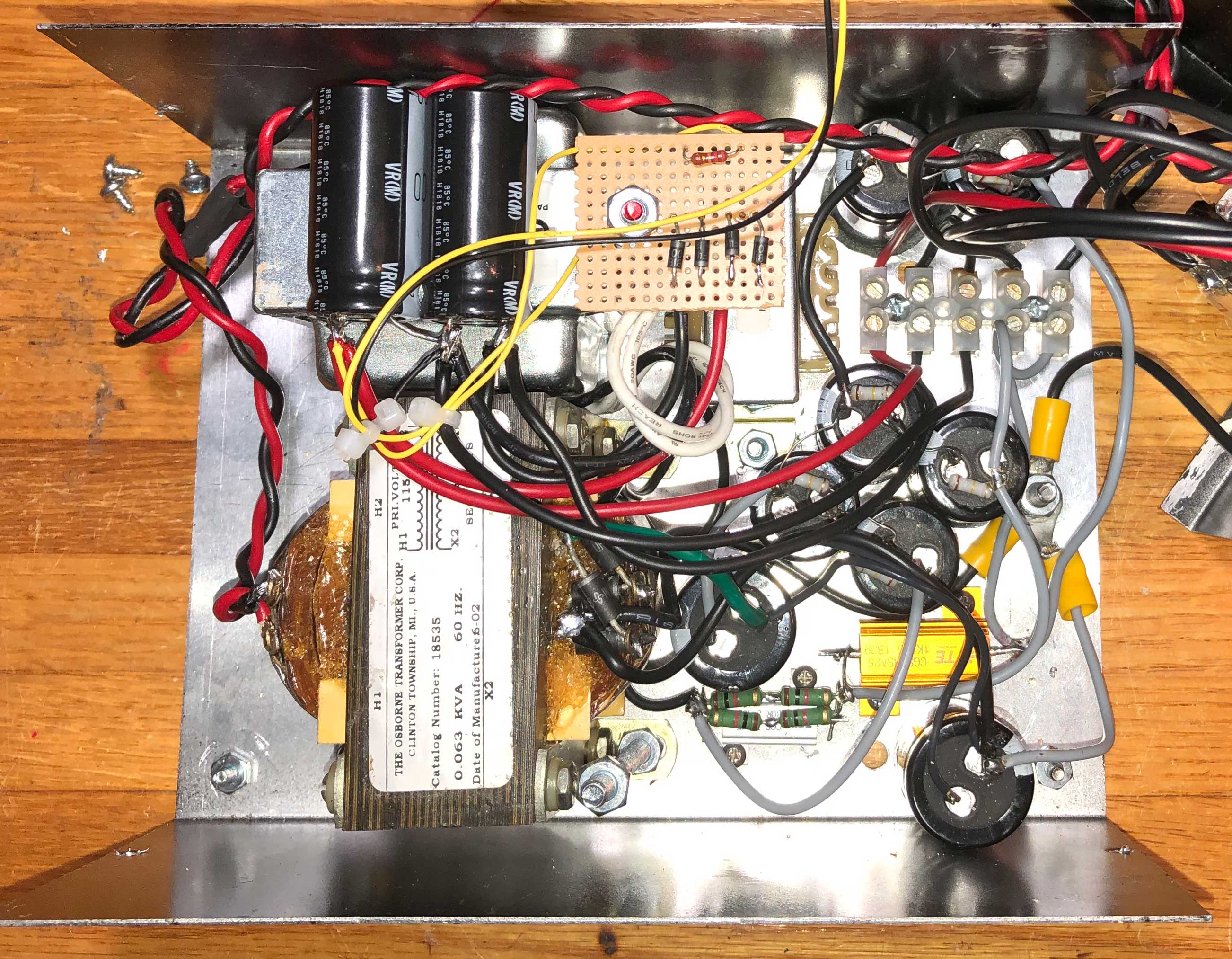
The completed raw PSU is shown below, opened up to reveal its guts.
VOLTAGE REGULATORS - abandoned due to REPEATED FAILURE
There are 2 250V regulators (one for each channel) and 2 180V regulators. I am using a very basic Maida-style regulator, first designed by Michael Maida in a 1980 National Semiconductor brief seen here. The basics of this circuit have been tweaked over the past 40 years, but the principles are the same. It uses a highly-accurate low-voltage IC regulator (LM317) to maintain a precise voltage as described below. Brilliant. A simple, but perfectly adequate implementation for the 180V regulators is shown below.
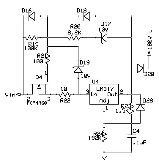
How does it work: The LM317 works by maintaining a dead-constant voltage of 1.25V between OUT and ADJ. Throw a 1.5K resistor between OUT and ADJ and you have a current of .8333ma. This current NEVER changes as long as the LM317 is regulating. So by adjusting R24, you can set the output voltage at an extremely constant value.
Unfortunately, the LM317 can't handle more than 40V across IN and OUT, so you need something in front of the LM317 to knock down the voltage. Enter the wonderful, high-gain, fragile N-channel MOSFET.
Take OUT and run it back to the gate of the MOSFET through a 10V zener D17. Ignoring R20 and R21 for now, the following holds:
IN = OUT + 10 - Vgs - 10I, where 10 is the value of R22, and I is the current through the regulator.
Assume Vgs = 5V, which is reasonable, then
IN = OUT + 5 - 10I.
If the current I hits 200ma, then IN = OUT + 3. The datasheet says that 3V is the dropout voltage of the LM317, so the regulator stops regulating when the current exceeds around 200ma.
4 of these regulator circuits are built, 2 for the 250V rails, and 2 for the 180V rails.
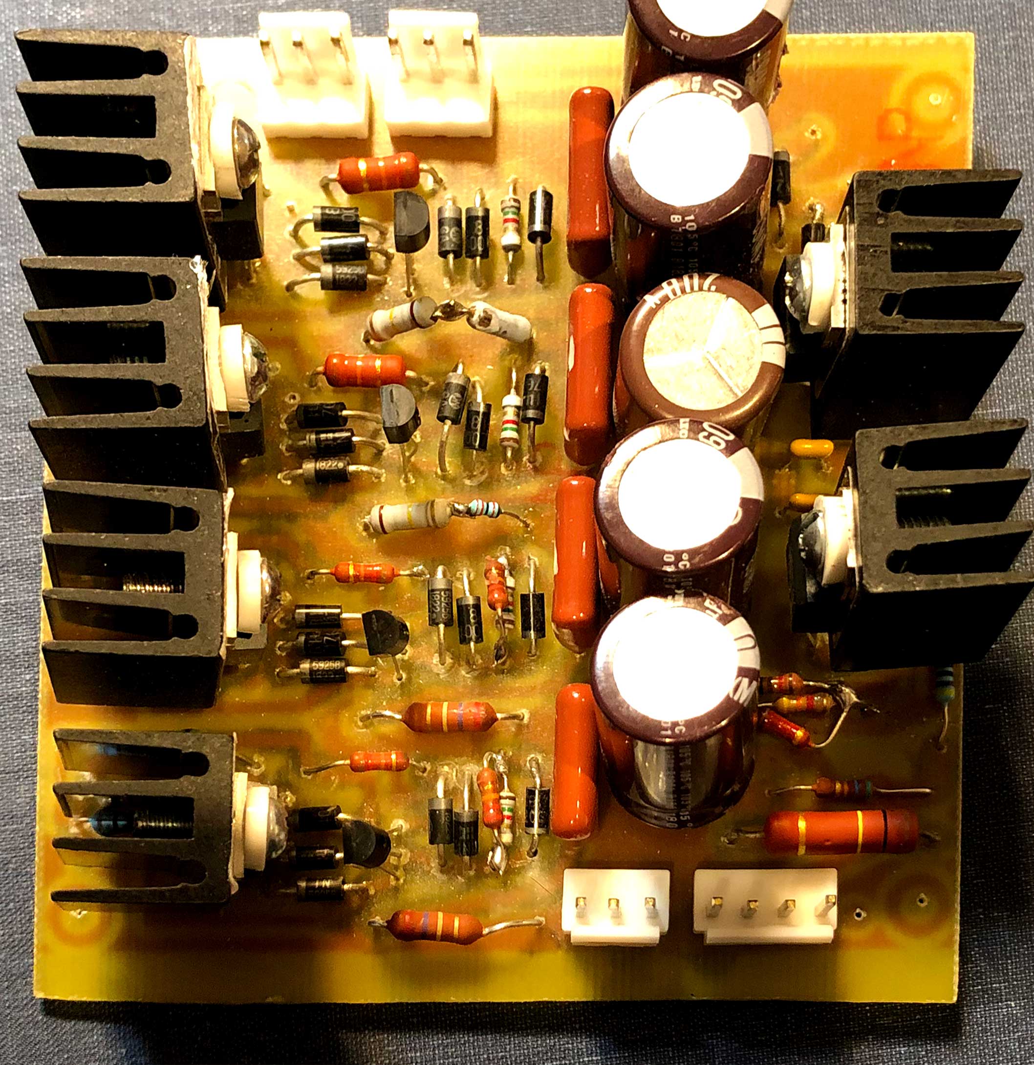
Below is the first Voltage Regulator Board. It is a DIY PC Board, stuffed with components. It's a little amateurish and rough-looking, but it works and is rock-solid, as I found out when I tripped on a wire coming off the board and flung it across the room.
The filament regulators are to the right, and the 250V and 180V regulators are to the left.
VOLTAGE REGULATORS - easier, more reliable, good enough
The little LM317's on the above board repeatedly failed and I never figured out why. I don't know if there were some weird voltage spikes on startup or what, but after hours of troubleshooting and lots of obscenities, I gave up on this design and decided to use an old, simpler design.
Below is the standard 2-transistor voltage regulator used for decades in tube amplifiers. Technically, it is not quite as good as the IC regulator based designs, but it's good enough here, particuarly since every amplifier circuit in this design is swimming in constant-current sources and sinks, affording excellent power supply rejection (PSRR).
There will be 4 of these circuits, 2 at 250V, 2 at 180V.
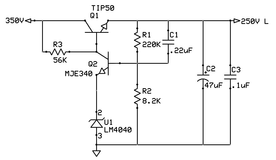
How does this one work: the voltage is set by the voltage reference U1 (shown as a zener). It sets a very constant voltage of 8.192V. There is a constant voltage of about .7 across the base-emitter junction of Q2. So R2 has about 8.9V across it at all times. This means a fixed current of 8.7/8.2 = 1.1ma. Ignoring Ib into Q2, R1 sees this same current, so
Vo = (220+8.2)*1.1 = 251V.
R3 is there to provide enough current to the voltage reference.
The pass transistor Q1 absorbs the shock of dropping the voltage from 350 to 250V, so it must be beefy enough to handle this drop across its collector-emitter junction and handle about 30-40ma current. The old reliable TIP50 fits the bill. It must be heat-sinked, though.
Any change in output voltage is sensed by Q2; if there is a drop in Vo, Q2 turns off a little, increasing the voltage at the base of Q1 and turning it on harder, allowing more voltage to pass through it, restoring the output voltage. The opposite occurs if there is an increase of Vout.
R1 is adjusted to produce 180V in the 180V regulators.
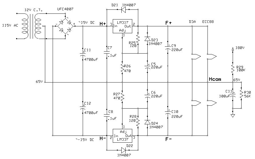
LOW-VOLTAGE HEATER POWER SUPPLY
The 6.3V filament supplies will also be regulated. This is a simple proposal, except for a twist.
The cathode voltage of the ECC88 cathode follower is on the order of 90V, and this means that the cathode to filament voltage will be about 90V, which exceeds the recommendations for this tube.
So the filament supply has to be elevated. If we elevate it to 65V, then the cathode to filament voltage of the cathode followers will be about 25V and the cathode to filament voltage of the other tubes will be about -65V, which is OK.
The regulators for the filaments are shown below.
Once again, the dependable LM317 and its negative voltage analogue LM337 are used. In this case, they can easily handle the 10V or so drop across them, so no MOSFET is necessary.
I designed a PCB to contain both the high-voltage and 6.3V regulators. I DIY'ed, stuffed it, fired it up, and it worked perfectly. Miracles never cease. It is shown below.